Look for General PCB Board? Find the definitions, benefits, applications, why choose the best technology as a PCB partner.
What is a common PCB board?
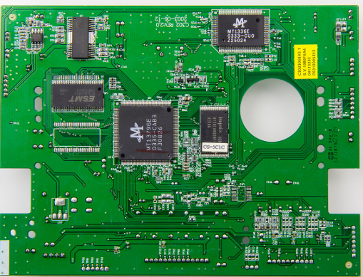
A A General PCB BoardReferring to standard print circuit boards that are widely used on various electronic devices. These boards are usually made from materials such as FR4 (fire-resistant epoxy laminated) and function as a foundation for installation and connecting electronic components. They are very important to create functional circuits in everything ranging from consumer electronics to industrial equipment.
What are the benefits of the general PCB board?
General PCB Board offers several benefits, including:
- Cost effective: They are affordable to be produced, making it ideal for mass production.
- Fabrication: Suitable for various applications throughout the industry.
- Reliability: Proven performance on various electronic devices.
- Ease of design and assembly: Easy to design and assemble, reduce production time.
- Durability: Material FR4 provides excellent mechanical strength and resistance to heat and humidity.
General PCB Board Application
PCB boards are commonly used in various industries, such as:
- Consumer Electronics: Smartphones, laptops and household appliances.
- Industrial equipment: Control system, sensor, and automation device.
- Automotive: Infotainment system, engine control unit, and lighting.
- Medical devices: Diagnostic equipment and monitoring systems.
- Telecommunication: Router, modem, and communication device.

How do I make a common PCB board prototype?
How to make a common PCB board prototype: 8 important steps
1. Scheme Design & Layout
- United States of America free/low -cost toolsLike Kicad, Easya, or Diptrace to arrange the layout of the circuit and PCB layout. Make sure the footprints components match the physical parts (for example, SOIC-14 vs DIP-14).
- For the tip: Include a 2 mm border around the edge of the board for routing and installation hole.
2.Produce Gerber File
- Industrial Standard Exports Gerber RS-274XBore and NC files. Verification of layers (copper, solddermask, silkscreen) using free performers (for example, gateview).
- Avoid: Hand sketch or non-standard format (for example, PDF) for fabrication.
3. Choose a prototype -friendly material
- Substrate: Select a FR-4 TG130â € “170Â for cost efficiency. Avoid high TG or Halogen free material unless required by design.
- Copper weight: Said 1oz (35 μm)For most prototypes’ thicker copper adds unnecessary costs.
4. Select the fabrication method
- Low -cost options: CNC routing for 1â € “5 pieces. Requires a manual front but avoiding the cost of tools.
- Balanced option: Ferric chloride or cupric chloride) for 5 € “20 boards. Use a laser printer toner transfer for the DIY project.
- Avoid: Laser cutting for thick copper (> 2oz) or tight tolerance (
5. Orders from shops that focus on prototypes
- Prioritize vendor offers 5 € “10 days of turnoverÂo treats There is no MOQ. Confirm they receive 2 layer boards 4 and standard finishing (Hasl/Enig).
- Red flag: Suppliers of fees for regulating fees for <50 pcs or refuse to review the pre-order gate.
6. Component assembly
- Solder Manual: Use the hot air re -work station for SMD spare parts (0402, QFN). Apply the solder paste with stencils or syringes.
- Automatic option: For> 50 pcs, consider local assemblers with pick-and-plate machines (cost $ 0.01â € “0.05 per bearing).
7. Test & Debug
- Visual inspection: Check the soldering bridge, tombstoning, or bearings raised under a microscope.
- Functional testing: Use a multimeter for continuity/shorts and signal generators for high frequency circuits.
- Repair: Crafts with braids that are desperate or pieces of pieces. Avoid excessive heat (> 300 ° C) to prevent removal of bearings.
8. Document iteration
- Label every revision of the prototype (for example, “Rev A1,” “rev A2 “) and track changes (for example,” Moved C1 is closer to U1 to reduce noise “).
- Tool: Use github or cloud storage to share gaters, bombs, and test results with team members.
Why choose the best technology for general PCB boards?
As a leader PCB manufacturer, Best Technology is your trusted partner for a high quality general PCB board. This is why:
- 18+ years of experience: With broad expertise, we provide a reliable and innovative PCB solution.
- Competitive price: We offer high quality products at the most affordable prices.
- There is no MOQ & Flexible option: Do you need a prototype or large -scale production, we accommodate all sizes of orders.
- 99% on time delivery: We make sure your project remains on schedule.
- ISO certified quality: Our manufacturing process is attached to ” ISO9001, ISO13485, and IATF16949‘Standard.
- Comprehensive service: From design to assembly, we provide a ” One -roof solutionFor all your PCB needs.
- Customer-centric approach: Our goal is “Total Customer Satisfaction”And we work with you to meet your needs.

How to reduce the cost of production of general PCB boards?
Optimizing the size & shape of the board
- Minimize dimensions: 10% reduction in the board area can reduce material costs by 15â € “20%. Use DFM tools for automatic components within tighter limits.
- Avoid special forms: Rectangular or square board waste fewer substrate than a circular/hexagonal design. Add post -production installation holes if needed.
Standardization of component placement
- Use general footprints: Prioritize the SOIC, QFN, and 00603 packages above BGA or QFP to reduce the complexity of the assembly.
- Reduce the number of layers: Combine the field of strength/land and reroute signals to eliminate unnecessary layers (for example, 4-lata â † 2-layer).
Leverage panelization efficiency
- Maximize the use of panels: Fill the gap with a smaller board or a doll coupon. The 500x600mm panel can load 40% more of 50x50mm boards with optimized nests.
- Adopt Score V.: Reducing the cost of labor ahead by 80% compared to stomach.
Negotiate material costs
- FR-4 Mass Purchase: Commit to a 6 month 6 month supply agreement for a 10% discount of 10%.
- Recycling memo: Partnering with local recycling to sell copper wrapped waste (usually $ 1â € “2/kg).
Automate production steps
- Invest in SMT Lines: Aâ 50Kâ € “100K Pick-and-Plase Machine reduces the assembly labor by 70% for> 1K unit/month.
- Use the AOI system: Optical Inspection Automatically cuts quality control costs by 50% vs. manual inspection.
Simplify the final surface
- Select Hasl Over Enig: Save 0.05 € “0.10 per board. Avoid gold for non-critical contact.
- Eliminate the mask that can be found: Use the stencil that is recorded instead to selective solder.
Outsourcing Non-Intic Process
- Couple for coating: Send a board to a specialist for Enig/Immersion Tin if the in-house regulation fee exceeds $ 20K.
- Use contract producers: For <500 pcs/month, the cost of cm (15â € "25% of the bomb fee) can compensate for the cost of labor/internal equipment.
Reduce the complexity of testing
- Limit the Flying Probe Test: Use bed equipment to run high volume (cost 500 € “1K but reduce testing time per unit by 60%).
- Pass the impedance test: Except designing for high -speed signals (for example, USB 3.0, HDMI).
Apply the Lean inventory
- Adopt jit (on time): Align component orders with a production schedule to avoid holding costs (usually 20-30% of the inventory value).
- Use the Kanban system: Re -order material when stock reaches 10â € “15% of the buffer level.
Our service
On Best TechnologyWe offer a variety of services for general PCB boards, including:
- PCB design: Special designs that are tailored to your specifications.
- PCB prototype: Fast and accurate prototypes to test your design.
- PCB manufacturing: High quality production with advanced technology.
- PCB assembly: Complete assembly service for smooth integration.
- Component source: Reliable high quality component sources.
- Testing and inspection: Strict testing to ensure performance and reliability.
Contact us today
For high quality general PCB boards, trust Best TechnologyAs your reliable partner. Contact us today to discuss the requirements of your project and get offers: [email protected].
Tag: General PCB Board
This entry was posted on æÿœœäº 27 5 月, 2025 at 6:10 ¸ ‹Å ˆ and submitted under the best PCB, BestTPCB, FR4 PCB. You can follow any response to this entry through RSS 2.0 bait. You can leave a response, or trackback from your own site.
Game Center
Game News
Review Film
Berita Olahraga
Lowongan Kerja
Berita Terkini
Berita Terbaru
Berita Teknologi
Seputar Teknologi
Berita Politik
Resep Masakan
Pendidikan
Berita Terkini
Berita Terkini
Berita Terkini
review anime
Gaming Center
Originally posted 2025-05-27 19:43:37.