SMT (Surface Mount Technology) is the dominant assembly method in modern electronics manufacturing, enabling compact and high-reliability products. Control SMT fundamentals and processes are critical to engineers, manufacturers, and buyers seeking consistent quality in electronic assemblies.
What is SMT?
SMT stands for Surface Mount Technology, a core electronics assembly process that mounts surface mount (SMD) components directly onto the surface of a printed circuit board (PCB). It replaces traditional through-hole technology, offering higher assembly density and production efficiency for most electronic devices.
Why Is SMT Widely Adopted?
- Enables smaller, lighter electronic products with a 40-60% volume reduction compared to through-hole designs.
- Supports high volume automation, cutting production costs by 30-50% in mass production.
- Provides better high frequency performance and lower electromagnetic interference (EMI).
Meaning of SMT
SMT is the abbreviation of Surface Mount Technology, referring to a set of techniques for mounting and soldering SMD on a PCB surface without drilling insertion holes. The core goal is to achieve reliable electrical and mechanical connections between components and PCB efficiently.
Key Terminology in SMT
- SMD: Surface Mount Device, components used in SMT assembly (resistors, capacitors, ICs, etc.).
- PCB: Printed Circuit Board, the basis for mounting SMT components.
- Reflow Soldering: A heating process that melts the solder paste to bond the SMD to the PCB pads.
Definition of SMT
Surface Mount Technology (SMT) is a standardized electronics assembly process that involves applying solder paste to PCB pads, precisely placing the SMD into the paste, and heating the assembly to form permanent solder joints. It is defined by IPC standards as a high-density automated assembly method for modern electronics.
Core Characteristics of SMT
SMT eliminates the need for drilling PCB holes for component wiring, relying on surface tension and solder paste adhesion to secure components. This results in lower PCB material usage, faster production cycles, and lower solder joint breakage rates compared to traditional methods.
What is SMT in Electronics
In electronics, SMT is the primary method for assembling PCBs in consumer devices, industrial controls, medical equipment, and communications hardware. This enables the miniaturization of high-performance electronic devices, from smartphones to 5G base stations.
SMT General Electronic Applications
- Consumer electronics: Smartphones, laptops, wearable devices, and televisions.
- Industrial electronics: PLCs, sensors and automation controllers.
- Medical devices: Diagnostic tools, wearable monitors, and imaging equipment.
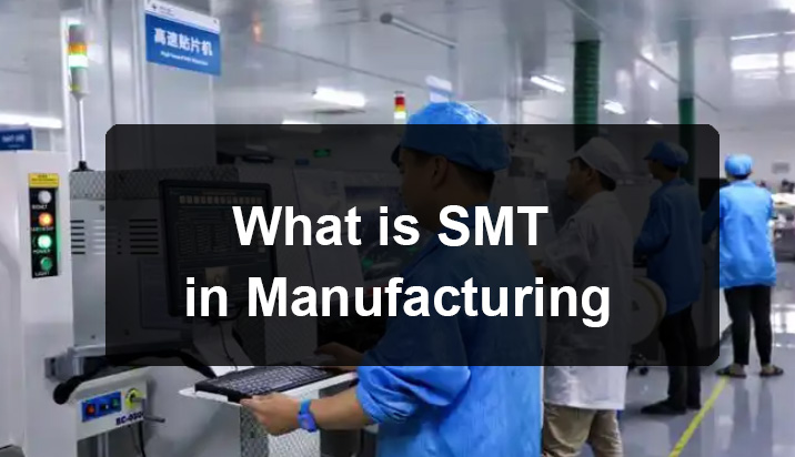
What is SMT in Manufacturing
In manufacturing, SMT is an efficient, automated process that integrates multiple stages—from solder paste printing to inspection—to produce consistent PCB assemblies on a large scale. This is the cornerstone of lean manufacturing for electronic components.
SMT Manufacturing Workflow Goals
- Achieve high throughput: Up to 30,000 parts per hour with advanced placement machines.
- Maintain low levels of damage: Target <10 ppm (parts per million) for critical applications.
- Ensure process repeatability: Complies with IPC-A-610 and IPC-7351 standards.
Basic SMT Process Flow
Basically SMT The process consists of 6 sequential stages, with each step directly affecting the quality of the final assembly. Front-end process control is critical to reducing defects and ensuring reliability.
What are the Core Stages of SMT?
- Solder Paste Printing: Apply solder paste to the PCB pads using a stencil, the first gate for welding quality. Laser cut stencils (precision ±5μm) and SPI (Solder Paste Inspection) are mandatory for high reliability projects.
- Component Placement: Use automatic machines to place SMDs onto solder paste, which requires a repeatability accuracy of ≤±25μm for 0201-sized components and fine pitch devices.
- Reflow Soldering: Heat the assembly to melt the solder paste, forming a permanent connection. Specific temperature profiles are required for different PCB thicknesses and component types.
- Inspection & Testing: Combine AOI (surface defects), X-ray (BGA/QFN bottom connection), and FCT (functional verification) to find hidden problems.
- Cleaning (Optional): Removes flux residues via water or semi-aqueous cleaning, tested to IPC-TM-650 for ion contamination.
- Improved Reliability: Implement ESD protection and underfilling for advanced packages to improve long-term stability.
SMT Placement Process
That SMT the placement process is a precision step that bridges solder paste printing and reflow soldering, having a direct impact on component alignment and solder joint integrity.
How to Ensure Accurate SMT Placement?
- Machine Calibration: Regularly calibrate the placement machine to maintain ±25μm repeatability accuracy, replace worn nozzles to avoid component slippage.
- Component Recognition: Use advanced vision systems to identify odd-shaped components and blackbody devices, thereby reducing placement errors.
- Double Sided Placement: For double-sided PCBs, prioritize lighter components first to prevent displacement during reflow.
- Real Time Monitoring: Integrates MES systems to track placement parameters, enabling immediate adjustments to offsets or misalignments.
Main Advantages of SMT Over Through-Hole Technology
SMT outperforms traditional through-hole technology in most modern electronics, offering irreplaceable benefits for miniaturization and mass production.
SMT vs. Through-Hole: Core Differences
| Metric | SMT | Through Hole |
|---|---|---|
| Component Density | 40-60% higher, enabling miniaturization | Low, limited by hole distance |
| Production cost | 30-50% lower in high volume manufacturing | Higher due to manual insertion |
| High Frequency Performance | Superior, lower EMI | Bad, lead inductance affects the signal |
Common SMT Defects and Troubleshooting Tips
Most SMT defects originate from process deviations in printing, placement, or reflow. Targeted problem solving reduces rework rates and increases consistency.
How to Fix Top SMT Defects?
- Open Connection/Vacancy: Adjusts the stencil aperture and reflow profile; ensure the freshness of the solder paste (shelf life ≤3 months).
- Bridge: Reduce the size of the stencil opening and optimize the printing pressure to avoid excess solder paste.
- Tombstone: Balance the solder paste volume on the component pad and adjust the placement accuracy to a pad offset of ≤1/3.
- cold soldering: Extend the reflow immersion time to fully activate the flux, ensuring peak temperature (240-250℃ for SAC305).
Important Factors for High Quality SMT Assembly
Achieve high quality SMT assembly requires a combination of equipment precision, process control and materials management, aligned with IPC standards.
What Drives SMT Assembly Quality?
- Material Control: Use low residue solder paste and ESD safe packaging for sensitive components.
- Process Documentation: Record SPI/AOI reports, X-ray images and reflow curves for full traceability.
- Operator Training: Certify staff regarding IPC-A-610 standards to identify and resolve minor process problems.
- Nitrogen Return Flow: Adopt nitrogen atmosphere for automotive/medical electronics to reduce oxidation and voids.
SMT FAQs
Below are general answers SMT questions, addressing issues in process optimization and quality control.
Frequently Asked Questions About SMT
- What is the acceptable void rate for SMT joints? Industrial-grade applications require a void rate of <25% for BGA/QFN components, tested via X-ray.
- How often should SMT stencils be cleaned? Clean the stencil every 50-100 prints to prevent paste buildup and blockage of openings.
- Can SMT handle double sided PCB? Yes—use low-temperature solder paste for the second side to avoid reflow of the existing joint.
- What is the difference between leaded and lead-free SMT? Lead-free (SAC305) requires a higher peak temperature (240-250℃) than lead (210-220℃).
- How to reduce SMT rework rate? Implement SPI on the front end—printing defects cause 70% of total SMT problems.
- Is undercharging necessary for SMT? This is mandatory for fine tone BGAs and automotive electronics to increase resistance to shock and vibration.
- What standards govern SMT assembly? IPC-A-610 (acceptance) and IPC-7351 (component land pattern) are industry benchmarks.
Future Trends of SMT Technology
SMT technology is evolving to meet the demand for advanced packaging, high reliability and intelligent manufacturing in 2026 and beyond.
What’s Next for SMT?
- Advanced Packaging Integration: Combines SMT with SiP/Chiplet technology for high-density, high-performance electronics.
- Smart Factory Adoption: Full integration of AI-based AOI, real-time process monitoring, and MES systems for data-driven optimization.
- Automotive Class Focus: Improves SMT for AEC-Q100/Q200 compliance, with improved thermal and vibration resistance.
- On-Demand Manufacturing: Flexible SMT line to support projects with low MOQ and fast turnaround for AIoT and wearable devices.
We provide high quality SMT assembly services, complying with IPC standards and advanced process controls to ensure the reliability of automotive, medical and industrial electronics. If you need it SMT the solution, order us today—contact via email at [email protected].
Tag: SMT Assembly Manufacturer, China SMT PCBA, electronic SMT applications, PCB board SMT, SMT PCB Assembly, SMD vs SMT, SMT, SMT Assembly, SMT Board Assembly, SMT defect troubleshooting, SMT in manufacturing, SMT PCB Assembly, SMT placement process, SMT PNP process, smt process, SMT process flow, SMT reflow process, SMT reliability, SMT solder paste printing
This entry was posted on Friday, January 23, 2026 at 14:58 and is filed under best PCB, best PCB, FAQ, Our News. You can follow any responses to this entry via the RSS 2.0 feed. You can skip to the end and leave a response. Ping is currently not allowed.
News
Berita Teknologi
Berita Olahraga
Sports news
sports
Motivation
football prediction
technology
Berita Technologi
Berita Terkini
Tempat Wisata
News Flash
Football
Gaming
Game News
Gamers
Jasa Artikel
Jasa Backlink
Agen234
Agen234
Agen234
Resep
Cek Ongkir Cargo
Download Film