Design and prototyping of one -sided printed circuit board is very important in electronic products. This blog aims to provide basic definitions, layers structure, benefits, standard production processes, and keys to improve the efficiency of the layout for one -sided printed circuit board.
As a technological sophisticated OEM supplier, the best technology provides the design and manufacture of one -sided printed circuit prototype for global clients. Quality is very important to gain our customer trust. Our PCB ranges include FR4 PCB, MCPCB, Ceramic PCB, and PCBA. We are the original factory that provides a fast turnover and high quality solution for you. Any side of the one -sided printed circuit board project, don’t hesitate to tell us on [email protected] And we will be happy to provide our best service to you.
Is that a one -sided printed circuit board?
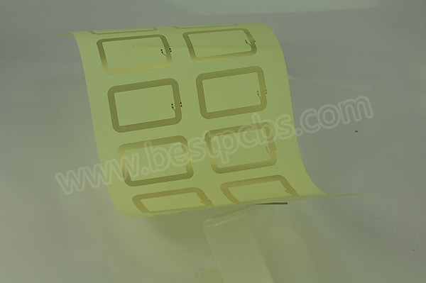
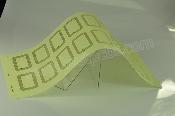
One -side printing circuit board (single side PCB) is the most basic PCB type, displaying conductive traces only on one side of the insulation substrate. Components are mainly mounted on the opposite side of the trace layer (or mounted on the same side), with an electric connection made through the soldering pads. Its core structure includes an insulation substrate (common materials such as FR-4, aluminum base, etc.) and one-sided copper foil layer, which is carved to form a specific circuit pattern. Thanks to the “One Lapis Cable” design, this PCB ensures basic electrical connectivity while significantly reduces the complexity and cost of manufacturing, making it a preferred choice for a simple electronic system.
One Side Print Circuit Stackup
Stackup (layer structure) Single side PCB is relatively simple, mainly consisting of two basic layers:
- The substrate layer isolation: Functioning as a circuit carrier, with common materials including the FR-4 epoxic glass fiber board (general use, cost-effective), aluminum substrate (very good heat discipline for power circuits), and paper substrates (low-cost, suitable for consumer electronics). Thickness usually ranges from 0.4mm to 3.2mm, selected based on mechanical strength and electricity performance requirements.
- One -sided copper foil layer: Includes one side of the substrate, with a standard thickness of 18îiefm (0.5oz), 35îief (1oz), and 70îief (2oz). This is engraved to form a conductive trail for current transmission and signal connection.
This single layer cable design limits the implementation of complex circuits but achieves an efficient balance between costs and performance through a reasonable track routing and component layout.
The core advantage of one -sided printed circuit board
- Low manufacturing costs: Eliminating complex processes such as multi-layer laminated and through coating, reducing material costs and processing by 30% -50% compared to multi-side/multi-layer boards, ideal for mass production.
- Short process cycle: Eliminating two -sided alignment and inner layer processing, allowing the shipping of prototypes as fast as 24 hours to accelerate product iterations.
- Solid reliability: Traces of one layer eliminate the risk of interlayer connection failure. After surface maintenance (such as HASL, OSP), they meet the long -term use requirements in the general environment.
- Low design threshold: Does not require complex interlayer signal coordination, suitable for the development of entry-level circuit and comfortable for manual solder and post-maintenance.
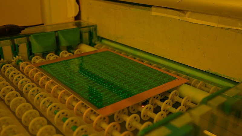
The process of production of one -sided printed circuit board
(1) Preparation of raw materials
- Material cutting: Cut the isolation substrate (for example, FR-4) to design dimensions with precision ± 0.1mm.
- Preprocessing Foil Copper: Clean the board wrapped in one -sided copper to eliminate surface oxidation and ensure optimal ETSA results.
(2) Circuit pattern formation
- Drilling: Use a CNC drilling machine to process the installation hole and position position with a diameter of ± 0.05mm.
- Transfer pattern: Transfer circuit design to the surface of the copper foil through exposure and the development of photoresists, with a minimum line/distance that can be controlled at 0.3mm/0.3mm.
- Etching: Remove the unprotected copper foil with a copper hydrochloric acid solution to maintain the right circuit pattern, with ETSA factor ‰ ¥ 1.5.
(3) Surface maintenance and processing
- Solder Mask Application: Mantle of green/black solder masks, exposure and developing to protect non-PAD areas, increase insulation and solder capabilities.
- Printing silkscreen: Mark component designers, polarity, and other information for easy assembly and maintenance.
- Finishing surface: Options include HASL, OSP, ENIG, etc., to meet different solder environmental requirements.
(4) quality control
- Electric testing: Use a flying probe or fixture test to ensure 100% conductivity trace and insulation resistance ‰ ¥ 100mî ©.
- Visual inspection: Combine the Visual Manual Inspection with AOI Equipment to check the traces of traces and mask solder defects, control the defect rate ‰0.1%.
One side printing circuit board application scenario
- Consumer Electronics: Calculator, Electronic Watches, LED Light Panels, etc., Utilizing Low Costs for Basic Function Integration.
- Industrial control: Small relay control board, sensor module, where a single layer cable meets the signal transmission needs and ensures stable operations in a hard environment.
- Education and R&D: Preferably for the university trial council and the manufacturing project, facilitating beginner understanding of the principles of the circuit and rapid prototype verification.
- Lower class equipment: Home appliance control boards (micro waves, electric fans), toy circuit boards, balance costs and reliability in low performance requirements.
Design considerations for one -sided printed circuit board
- Stomach tracker: Avoid the right corner turn (reduce signal reflection), prioritize the stomach throughout the alignment of the component, and complete the complex crossover through a detour or jumper.
- PAD Design: Make the diameter of PAD through a hole 0.2-0.4mm greater than the PIN diameter; Follow the component data sheet for the SMD pad size to prevent cold solder or short circuit.
- Land maintenance: Use large ground copper to reduce soil impedance; Avoid signal loops across soil separation to improve anti-interference capabilities.
- Component layout: Place high power components (for example, resistors) from components that are sensitive to heat (for example, capacitors); Separate the SMD and ENT components to optimize the soldering process.
The choice of thickness for one -sided printed circuit board
The single side PCB thickness range is usually 0.4mm-3.2mm, with selection based on:
Mechanical strength: Thin board (0.4-1.0mm) for portable devices that are limited to space; Thick board (1.6-3.2mm) for industrial applications that support heavy components.
Heat Discussion: Aluminum-based Single PCB (thickness 1.0-3.0mm) with thick copper foil (for example, 2oz) increases heat efficiency for power circuits such as LED drivers.
Electricity Performance: Creepage distance for high voltage isolation (for example, medical device power board) is determined by the distance of the conductor and surface coating, with compliance with inhibition of flames depending on the selection of substrate material.
Our service-complete process, one-stop solution
As a PCB manufacturer with 19 years of experience, we offer professional services throughout the product life cycle:
- Design support: The senior engineer team helps with DFM examination to optimize the layout and process feasibility, reduce the risk of prototyping.
- Fast prototype: One-sided PCB prototype is available as fast as 24 hours, with online bookings and real-time production tracking.
- Mass production: Some automatic paths support the monthly capacity of 5000ãž, strictly comply with the standard IPC-A-600 for batch consistency.
- Assembly services: Providing one -roof SMT (down to 0402 components) and ENT assembly, including functional testing and delivery of finished products.
Manufacturing Ability – Hardcore Process, Guarantee of Strength
| Goods | Ability parameter |
| Number of layers | Single layer (exclusive for one -sided PCB) |
| Substrate material | FR-4, aluminum base, copper base, paper substrate, CEM-1, etc. |
| Copper foil thickness | 18îlen (0.5oz), 35î¼m (1oz), 70old (2oz) |
| Minimum width/distance | 0.3mm/0.3mm (standard), support 0.25mm/0.25mm (special process) |
| Finishing surface | Hasl (Pb/Lead Free), OSP, Enig, Tin Soaking, Silver, Golden Finger Coating, etc. |
| Dimensional range | Minimum 50mmã-50mm maximum 1000mmã-600mm |
| Hole processing | Mechanical drilling (a minimum hole diameter of 0.3mm), Supporting Countersunk Hole, Blind Vias (Only Metalization Single Side) |
Why choose us? – 19 years of expertise, built on trust
- Accumulated: Serving more than 100,000+ clients in 20+ industries including communication, industrial control, and consumer electronics, with in -depth insights about the pain point of the one -sided PCB process and optimization.
- Sophisticated equipment: Imported German Etsa Line and AoO AoI detector America is full of America, controlling the accuracy of the main process in ± 5%, higher than the average industry.
- Tight quality control: ISO9001: 2015 and IATF16949 Certified, with Rohs Compliance Reports for each Batch Material and Factory Graduation Rate ‰ ¥ 99.9%.
- Flexible response: Supports low volume production (minimum 10 pieces) and accelerates urgent orders, with a technical consultation of 7ã -24 and after -sales support.
The problem resolved with one -sided printed circuit board
- Simple circuit implementation: Eliminating the need for complex multi-layer designs, completing the basic signal connection through a single layer cable € “ideal for low/medium volume projects that are sensitive to the cost to shorten the time-to-market.
- Reducing maintenance difficulties: The component is located at the center on the one hand (or clearly separated), allows the location of intuitive errors and convenient manual repairs, significantly reduces post-sales maintenance costs, especially for devices with high-sales dependence.
Place your order today – 19 years of process expertise, maintaining your circuit
Good for the first prototype of startup or mass production of mature projects, we provide professional processes and efficient services to turn on your circuit design. Contact us and send your needs directly to [email protected] For adjusted offers and technical solutions. Let the simple design of PCB one side into a reliable foundation of the competitiveness of your product!
Tags: Design and prototyping of one -sided printed circuit board, one -sided printed circuit board
This entry was posted on Friday, May 30, 2025 at 14:52 and submitted under the best PCB, BestTPCB. You can follow any response to this entry through RSS 2.0 bait. You can leave a response, or trackback from your own site.
Game Center
Game News
Review Film
Berita Olahraga
Lowongan Kerja
Berita Terkini
Berita Terbaru
Berita Teknologi
Seputar Teknologi
Berita Politik
Resep Masakan
Pendidikan
Berita Terkini
Berita Terkini
Berita Terkini
review anime
Gaming Center
Originally posted 2025-06-01 20:28:25.