The Multilayer PCB design is the heart of a compact high -speed electronics. Because more devices require higher functionality in smaller packages, multilayer PCB has become an entry solution. In this blog, we will explore how this board is designed, what materials are included in it, and how they are produced.
The best technology is a trusted PCB manufacturer based in China, which is specialized in small to medium PCB fabrication, PCB assembly, and comprehensive electronic manufacturing services (EMS). As a one -stop PCB solution provider, we surpass manufacturing. Our services include Turnkey assembly, component sources, box assembly, PCBA testing, and full electronic assembly. Whether you develop a prototype or increase full production, the best technology is committed to providing reliable quality, fast turnover, and personalized support to meet all your PCB and electronic manufacturing needs.
What is Multilayer PCB?
Multilayer PCB is a type of printed circuit board that is made by accumulating several copper layers with insulation material in between. While one -sided PCB only has one conductive layer and two -sided PCB has two, multilayer PCBs usually begin in four layers and can exceed thirty layers depending on the complexity of the design.
This copper layer is interconnected using VIAS (small -layered hole). The main advantage is that Multilayer PCB allows more complex circuits in compact form. They are used when simple stomachs become impossible because of high component density, high -speed signals, or design restrictions.
Multilayer boards usually contain a layer of signals, power aircraft, and soil fields that are arranged symmetrically to ensure electrical balance and mechanical stability.
The advantages of the multilayer PCB
There are many advantages of Multilayer PCB, especially for high -class applications, compact, and performance -based:
- High circuit density: PCB Multilayer offers more real estate by using many layers. This helps to repay more connections without crowding.
- Compact size: With a buildup of layers, complex circuits can be condensed into smaller board sizes, which are important for modern gadgets.
- Better signal integrity: plane and plones protect the signal layer, helps reduce electromagnetic disorders and signal loss.
- Increased reliability: Because many connections are internal and automatic PCBs, multilayer tends to be more reliable than manual cable boards.
- Increased power distribution: Special electricity packages help distribute power evenly throughout the board.
- Cost efficiency in mass production: although more expensive to be designed, they become cost effective when produced on a scale.
What material is used for Multilayer PCB?
Multilayer PCB construction involves several materials selected based on electricity, thermal, and mechanical application requirements. General ingredients include:
- Copper foil: Used for all conductive layers. Thickness ranges from 0.5 oz to 3 oz, depending on the current requirements.
- Core Material (FR4): The most widely used substrate, made from epoxy that is strengthened by fiberglass. This provides strength and mechanical insulation.
- Prepreg (Pre-Import Resin): Fiberglass that is impregnated with resin that binds the shared layer during lamination.
- High frequency material: For applications such as 5G or RF circuits, materials such as PTFE, Rogers, or Ceramic Substrates are used.
- Solder mask: This green or colored layer protects the board from the oxidation bridge and solder.
- Silkscreen: Printed on the board to mark the position and component label.
For high temperature applications or high reliability, alternative materials such as polyimide or metal core can also be used.
Why is there no 3 -layer PCB?
Technically, you can make PCB 3-Lapis, but they are not very common and are often impractical. PCB Manufacturing is designed to support the layer configuration numbered even for several reasons:
1. Symmetry: Stack-ups that are even layered offer a better mechanical balance. Strange layers can cause warping boards due to uneven internal pressure.
2. The simplicity of manufacturing: Most production paths are optimized for 4, 6, or 8 layers. The 3-lapi board will require a special process, which increases costs.
3. Signal performance: High -speed signals benefit from symmetrical structures. Odd-layer design makes it more difficult to maintain signal and power integrity.
For this reason, designers usually move to 4-lairis design when they exceed the two-sided layout.
How to design a multilayer PCB?
Designing a multilayer PCB begins with understanding the functional needs of your product. This is the step by step process:
- Determine the number of layers: Decide how many layers are needed based on the complexity of the circuit, signal integrity, and available space. General configurations include 4, 6, and 8 layers.
- Create a pile: Plan how each layer will function-signal, ground, or power. Setting the layer impact on EMI’s performance and routing efficiency.
- Placement of components: Place high-speed components, sensitive, and carefully. Separate the analog and digital parts.
- Routing Strategy: Critical signal route in the inner layer to protect them from external noise. Use short and direct routes for clock and high -speed paths.
- Via planning: Use VIAS through holes, blind Vias, and Vias buried to connect different layers.
- Impedance Control: For high -speed signals, calculate and control track impedance using PCB design software.
- Thermal management: Add thermal Vias and consider pouring copper for better heat distribution.
- Design for Production (DFM): Make sure the width of the trail, distance, hole size, and permission to follow the producer guidelines.
Design tools such as Altium Designer, Eagle, or Kicad can help streamline the Multilayer PCB design when checking errors along the road.
How do I build a Multilayer PCB pile?
Stacks are regulating copper and dielectric layers on Multilayer PCB. This affects the quality of signals, EMI, thermal behavior, and mechanical strength.
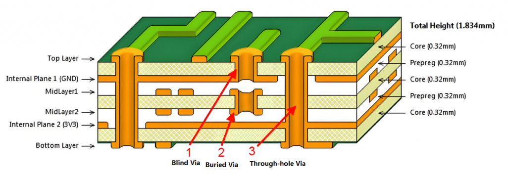
Piles of 4-laspi General:
- Upper layer: signal
- Inner layer 1: soil
- Layer in 2: strength
- Lower layer: signal
Examples of 6-layer buildup:
- Top: signal
- Layer 2: soil
- Layer 3: signal
- Layer 4: signal
- Layer 5: strength
- Below: signal
Tips for Effective Piles:
- Keep the soil layer and the power close for decoupling.
- Place a critical signal between the land field.
- Symmetry reduces warping.
- Maintain consistent dielectric thickness to control impedance.
In the best technology, our technical team helps clients with stack-up planning to match their performance, size, and target fees.
Multilayer PCB Manufacturing Process
The process of making a multilayer PCB involves combining several layers of copper and isolation through the right steps:
1. Internal layer imaging
Each internal copper layer is printed with the desired circuit pattern using a photoresist and UV lamps.
2. ETSA
Unwanted copper chemically engraved, leaving only a trail of the circuit.
3. Lamination
All layers are stacked with Prepreg between them and laminated under the heat and pressure to form a single board.
4. Drilling
The hole is drilled through a pile to connect the layer. This is included through holes, blind, and buried.
5. Plating
Copper is coated into a drilled hole and on the surface of the board to make an electric line.
6. Imaging and outer layer etc.
The outer layer undergoes the same photoimaging and etching processes as the inner layer.
7. Solder and Silkscreen Mask Applications
Solder mask is added to prevent oxidation and short circuits. Silkscreen is printed for component labeling.
8. Surface finishing
The final results such as HASL, ENIG, or OSP are applied to pads for better solderability.
9. Testing and Inspection
Each board underwent electricity tests and visual inspections to capture defects.
In the best technology, we combine automatic optical inspections (AOI), flight probe testing, and impedance measurement tools to ensure product quality at each stage.
Multilayer PCB Application
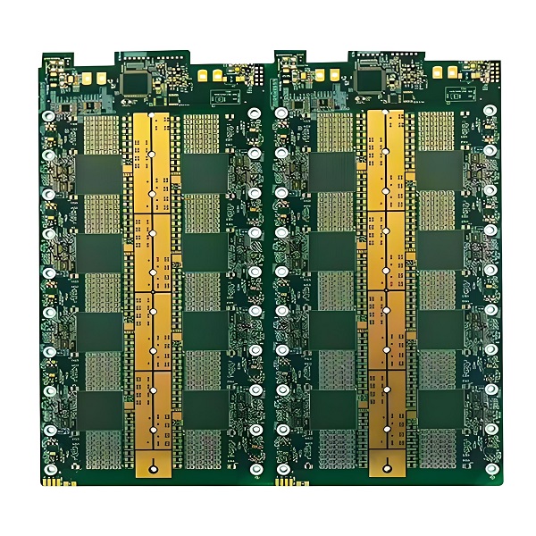
Multilayer PCB is used in products where performance and miniatures are very important. Here are some typical Multilayer PCB applications:
- Smartphones and tablets: compact devices require a high density PCB to match the advanced features in a tight space.
- Medical equipment: imaging machine, heart monitor, and portable diagnostic device depend on a stable multilayer circuit.
- Automotive Electronics: Modern vehicles use Multilayer PCB for infotainment, sensor, and control unit systems.
- Telecommunications devices: Routers, switches, and 5G antennas rely on multilayer design for signal integrity.
- Industrial Control: Automation Equipment Support PCB Multilayer and High Voltage Circuit.
- Military and Aerospace: Satellites, Drones, and Radar Systems require a strong multilayer board with very good thermal performance and electricity.
How to identify Multilayer PCB?
Identifying Multilayer PCB can be complicated just by looking at the surface. However, here are some tips:
- Edge Display: Under the magnifying, you can often see several stacked layers on the edge of the board.
- X-ray inspection: In the factory, X-ray equipment can show internal connections and VIAS is not visible from the outside.
- Blind/buried VIAS: If the board has a VIAS that does not go through the entire thickness, there is a possibility of many multilayers.
- Complexity and component density: compact boards that handle many components usually suggest multilayer design.
FAQ
1. How many typical layers in Multilayer PCB?
Most common, Multilayer PCB has 4, 6, or 8 layers. Upper class design can reach 32 or more.
2. Can PCB Multilayer Flexible?
Yes. Flexible Multilayer PCB is used in applications that can be worn, cameras, and aerospace where bending is needed.
3. Are Multilayer PCBs expensive?
The price is more than a single PCB or a double layer but offers more values in saving space and performance.
4. What is the difference between blind and buried?
Blind Vias connects the outer and inner layers. Buried only connects the internal layer, and hidden from the surface.
5. How is the best technology supporting the Multilayer PCB project?
We offer complete support support, pile suggestions, high-speed materials, and full tracking through the MES system.
Tags: Advantages of Multilayer PCB, Multilayer PCB Making Process
This entry was posted on Friday, May 30, 2025 at 17:19 and submitted under the best PCB, BestTPCB, Design Guide, FAQ, PCB News. You can follow any response to this entry through RSS 2.0 bait. You can leave a response, or trackback from your own site.
Game Center
Game News
Review Film
Berita Olahraga
Lowongan Kerja
Berita Terkini
Berita Terbaru
Berita Teknologi
Seputar Teknologi
Berita Politik
Resep Masakan
Pendidikan
Berita Terkini
Berita Terkini
Berita Terkini
review anime
Gaming Center
Originally posted 2025-06-01 08:20:29.