What is Silkscreen on PCB?
Silkscreen on a PCB is a layer of printed markings used to display component names, polarity markings, Pin 1 indicators, test points, logos, warning labels, QR codes, and board revision information. This helps engineers, assemblers, inspectors and repair technicians understand PCBs faster.
This layer is also called the PCB legend layer or component marking layer. It does not conduct current, but plays a practical role in assembly accuracy, test efficiency, repair work and product traceability.
Why is Silkscreen Important on PCBs?
PCB silk screens are important because they turn blank circuit boards into readable engineering documents. Without silkscreen, the board may still function electrically, but assembly, inspection, testing, and repair are slower.
Clear markings help identify resistors, capacitors, ICs, connectors, test points, power input, signal direction and safety warnings. In production, a clean silkscreen can reduce orientation errors, shorten debugging time, and improve communication between design, fabrication, and PCB assembly teams.
What is Silk Screen PCB Material?
Silkscreen PCB material usually refers to the ink or marking medium used to print text, symbols, and images on the PCB surface. The most common materials are non-conductive epoxy inks or UV-curable inks. These materials were chosen because they adhere to the solder mask, withstand normal handling, and remain readable after PCB fabrication.
In standard PCB manufacturing, the silkscreen material must be compatible with the solder mask color, curing temperature, surface finish, cleaning process, and assembly environment. For more demanding products, such as industrial electronics, automotive modules, medical PCBs, or outdoor devices, marking materials must also provide greater resistance to abrasion, chemicals, humidity, and temperature changes.
What are the Common Types of Silkscreen PCB Materials?
Different silkscreen PCB material options are used depending on cost, readability, board density, and traceability requirements. Common standard epoxy ink for most FR4 PCBs. UV-curable inks are used when faster drying and sharper printing are required. Laser marking is often chosen for durable QR codes, serial numbers and traceability marks.
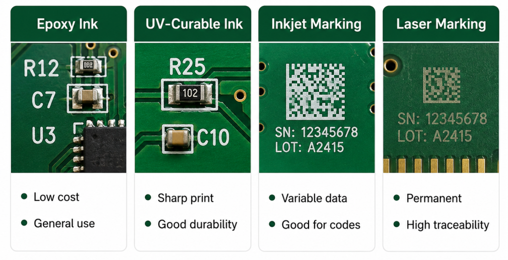
For general PCB projects, standard white or UV epoxy ink is sufficient. For small text, QR codes, high-density boards, or products that require long-term tracking, higher resolution printing or laser marking may be a better choice.
How Does Silkscreen PCB Material Affect Readability and Durability?
The silkscreen PCB material affects how sharp, visible, and durable the printed sign is. Good materials should keep the letters clean after curing, cleaning, soldering, handling, and final assembly.
If the ink spreads too much, small characters may appear blurry. If the ink adhesion is weak, the markings may fade or scratch. If color contrast is poor, technicians may have difficulty reading the board during inspection or repair.
For example, the white silk screen on the green solder mask is easy to read. The black silk screen on the white solder mask also provides strong contrast. But low-contrast combinations, such as gray text on a black solder mask, may look stylish while reducing practical readability.
What Are Silk Screen PCB Symbols?
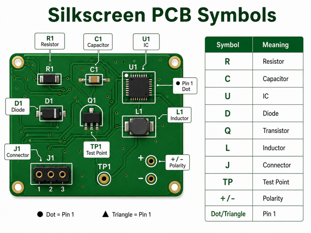
Silkscreen PCB symbols are printed markings used to identify components, polarity, Pin 1 direction, test points, connectors, warning areas and functional zones on a circuit board. These symbols help users understand the board without opening the schematic every time.
Common silkscreen PCB symbols include “+” and “-” for polarity, a dot or triangle for Pin 1, diode bars for cathode direction, TP labels for test points, and reference markings such as R, C, U, D, J, L, Q, and F.
What Do Common PCB Silkscreen Symbols Mean?
| Silk Screen PCB Symbols | Meaning | Example |
|---|---|---|
| R | Inhibitor | R1, R25 |
| C | Capacitor | C3, C18 |
| U/IC | Integrated circuits | U1, IC2 |
| D | Diode or LED | D5, LED1 |
| Q | Transistor or MOSFET | Q2, Q10 |
| L | Inductor | L1, L4 |
| J/CN | Connector | J1, CN3 |
| F | Fuse | F1 |
| etc | Test point | TP1, TP_GND |
| SW | Divert | SW1 |
| + / – | Polarity | Capacitors, batteries, LEDs |
| Dot / triangle / “1” | Pin 1 indicator | IC or connector orientation |
| GND | Land | Ground test point |
| WINE / VOUT | Power input/output | Power connector marking |
| H.V | High voltage warning | Power supply board |
These silkscreen PCB symbols are small in size, but carry important information. Missing polarity markings or unclear Pin 1 indicators can cause assembly errors, especially on LED boards, power supplies, sensor modules, and control boards.
How Do Silkscreen PCB Symbols Help Assembly?
Silk screen PCB symbols help assembly teams place and inspect components correctly. They show the location of each component, which direction it should go, and how the connector or test point should be used.
For SMT assembly, symbols such as Pin 1 dots, diode direction marks, and capacitor polarity marks are very useful during the first item inspection. For through-hole assemblies, connector names, switch labels, and power markings help manual operators avoid installation errors.
In PCBA production, clear symbols can support:
- Faster visual inspection
- Lower risk of component misorientation
- Connector installation is easier
- Better manual soldering guide
- Faster functional testing
- Repairs and troubleshooting are easier
What are the Design Rules for Silkscreen on PCBs?
Silkscreen on PCBs must be designed with sufficient character size, stroke width, and pad clearance. Markings must remain legible after fabrication and assembly.
| Design Items | Recommended Value |
|---|---|
| Text height | ≥1.0 mm / 40 million |
| Stroke width | ≥0.15 mm / 6 mil |
| Clearance to bearings | ≥0.15 mm / 6 mil |
| Clearance for open copper | ≥0.15 mm / 6 mil |
| Hollow font height | ≥1.5 mm / 60 million |
| QR code size | Confirm with the supplier |
| Bottom side text | Correctly reflected |
If the board is very dense, do not force every component label on the PCB. Save the important markings first: Pin 1, polarity, test point, connector name, warning label and revision number.
Can Silkscreen be Printed on Pads or Vias?
Silk screen should not be printed over solder pads, exposed copper, gold fingers, test points, or solderable vias. If the silkscreen covers these areas, the PCB manufacturer may remove some of the text during CAM processing.
This is why some letters disappear after being created. The original design may display the full text, but the manufacturer’s file may truncate it to protect soldering quality.
A better practice is to place reference markers outside the component body and away from the pad. For small components, use shorter labels or place complete reference information on the assembly drawing.
What is the Difference Between Silkscreen PCB Material and Solder Mask Material?
Silkscreen PCB material is used for printed marking. Solder mask material is used to protect copper and prevent solder bridges. They are different layers with different functions.
| Goods | Silk Screen PCB Material | Solder Mask Material |
|---|---|---|
| Main function | Print text, symbols and logos | Covers and protects copper |
| The role of electricity | Non-conductive marking | Insulation protection |
| General color | White, black, yellow | Green, black, blue, red, white |
| Used for | Component labels, symbols, warnings | Soldering control and copper protection |
| Design concerns | Readability and permissions | Insulation and solderability |
PCBs require a solder mask for manufacturing protection. Silkscreen is used to make it easy for humans to read. Both layers support production quality, but they should not be confused.
How Should You Choose Silkscreen PCB Material and Color?
Select silkscreen PCB materials and colors based on readability, product environment, board density, and traceability requirements. For most PCB projects, white silk screen on green solder mask is the safest and most readable choice.
For white solder mask, black silkscreen is usually better. For black solder mask, white silkscreen provides better contrast. For products with QR codes, serial numbers, or long-term tracking needs, laser marking or high-resolution legend printing may be more reliable.
| PCB Solder Mask Color | Recommended Silk Screen Colors | Legibility |
|---|---|---|
| Green | White | Very good |
| Blue | White | Very good |
| Red | White | Good |
| Black | White | Good |
| White | Black | Very good |
| Yellow | Black | Good |
For industrial, medical, automotive and communications products, readability should be more important than visual decoration. Beautiful boards are helpful, but easy-to-read boards are more useful in production and maintenance.
How Can EBest Circuits Help Silkscreen PCB Design and Manufacturing?
EBest Circuits can help review silkscreens on PCBs before fabrication and assembly. Our team checked text size, symbol clarity, polarity markings, Pin 1 indicators, pad spacing, QR code position, and board revision information during the DFM review.
This is very useful for turnkey PCB and PCBA projects. Silkscreen is not just a printing detail. This connects to BOM verification, component orientation, assembly inspection, testing, traceability, and repair documentation.
EBest Circuit Support:
- PCB fabrication
- PCBA assembly
- Component source
- Free DFM review
- Silk screen readability check
- QR code and serial number marking
- AOI, X-ray, ICT, and functional testing
- Prototype for mass production support
For projects that require clean markings, stable assembly and traceable production, send your Gerber files and BOM to [email protected].
FAQs
1. What is silkscreen on PCB?
Silkscreen on a PCB is a layer of printed markings that shows component names, symbols, polarity, test points, logos, QR codes, and board revision information. It helps people assemble, test, inspect and repair PCBs more easily.
2. What materials are used for PCB screen printing?
Common silkscreen PCB materials include epoxy-based inks, UV-curable inks, LPI legend inks, inkjet marking inks, or laser marking depending on the required precision, durability, and traceability.
3. What do the silk screen PCB symbols mean?
Silk screen PCB symbols identify the components and functions of the board. For example, R means resistor, C means capacitor, U means IC, D means diode, TP means test point, and “+ / -” indicates polarity.
4. Does silkscreen PCB material affect circuit performance?
Usually, no. Silkscreen material is non-conductive and does not conduct current. However, poor placement of pads, exposed copper, or sensitive areas can cause production or readability problems.
5. Can PCB silkscreen symbols be customized?
Yes. Custom symbols, logos, connector labels, warning signs, QR codes and product IDs can be printed on PCBs as long as they meet the manufacturer’s minimum size and clearance regulations.
6. What is the best silkscreen color for PCB?
White is the most common silkscreen color because it provides a strong contrast to the green, blue, red, and black solder masks. Black silk screen is usually better for white solder mask.
Tags: PCB silkscreen colors, Silkscreen on PCB, silkscreen PCB materials, silkscreen PCB symbols
This entry was posted on Friday, May 8, 2026 at 18:02 and is filed under best PCB, best PCB, FAQ, FR4 PCB, PCB News. You can follow any responses to this entry via the RSS 2.0 feed. You can skip to the end and leave a response. Ping is currently not allowed.
PakarPBN
A Private Blog Network (PBN) is a collection of websites that are controlled by a single individual or organization and used primarily to build backlinks to a “money site” in order to influence its ranking in search engines such as Google. The core idea behind a PBN is based on the importance of backlinks in Google’s ranking algorithm. Since Google views backlinks as signals of authority and trust, some website owners attempt to artificially create these signals through a controlled network of sites.
In a typical PBN setup, the owner acquires expired or aged domains that already have existing authority, backlinks, and history. These domains are rebuilt with new content and hosted separately, often using different IP addresses, hosting providers, themes, and ownership details to make them appear unrelated. Within the content published on these sites, links are strategically placed that point to the main website the owner wants to rank higher. By doing this, the owner attempts to pass link equity (also known as “link juice”) from the PBN sites to the target website.
The purpose of a PBN is to give the impression that the target website is naturally earning links from multiple independent sources. If done effectively, this can temporarily improve keyword rankings, increase organic visibility, and drive more traffic from search results.