What Copper PCB naked? Let’s explore the benefits, applications, design guides, design specifications, manufacturing processes, manufacturer selection methods.
Are you worried about this problem?
- Is your device too hot and slowdown? â € “Does the traditional FR-4 board always force you to prioritize cooling under high load?
- Is the generation high in the small space? “In catching thinness and lightly, is the performance or reliability sacrificed because of insufficient heat dissipation?
- Is the cost of cooling difficult to control? â € “Does add heat sink and fans increase bomb costs with limited effectiveness?
The best technology can provide solutions
- Metal-based thermal conductivity: Aluminum/copper substrate offers a thermal conductivity of 5-10 times higher, allowing rapid heat dissipation and stable surgery in a high temperature environment.
- Compact design: Integrated metal -based mold eliminates the need for additional heat discipline components, increasing space use by 30%.
- Total Cost Optimization: Reducing procurement and assembly costs for the cooling module, reducing the overall life cycle cost by 20%.
Welcome to contact us if you have a request for PCB Base Copper: [email protected].
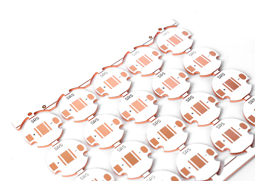
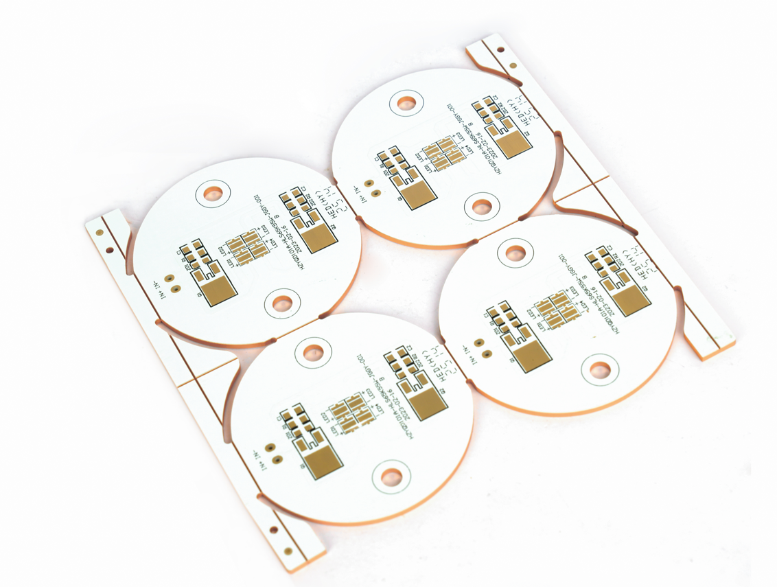
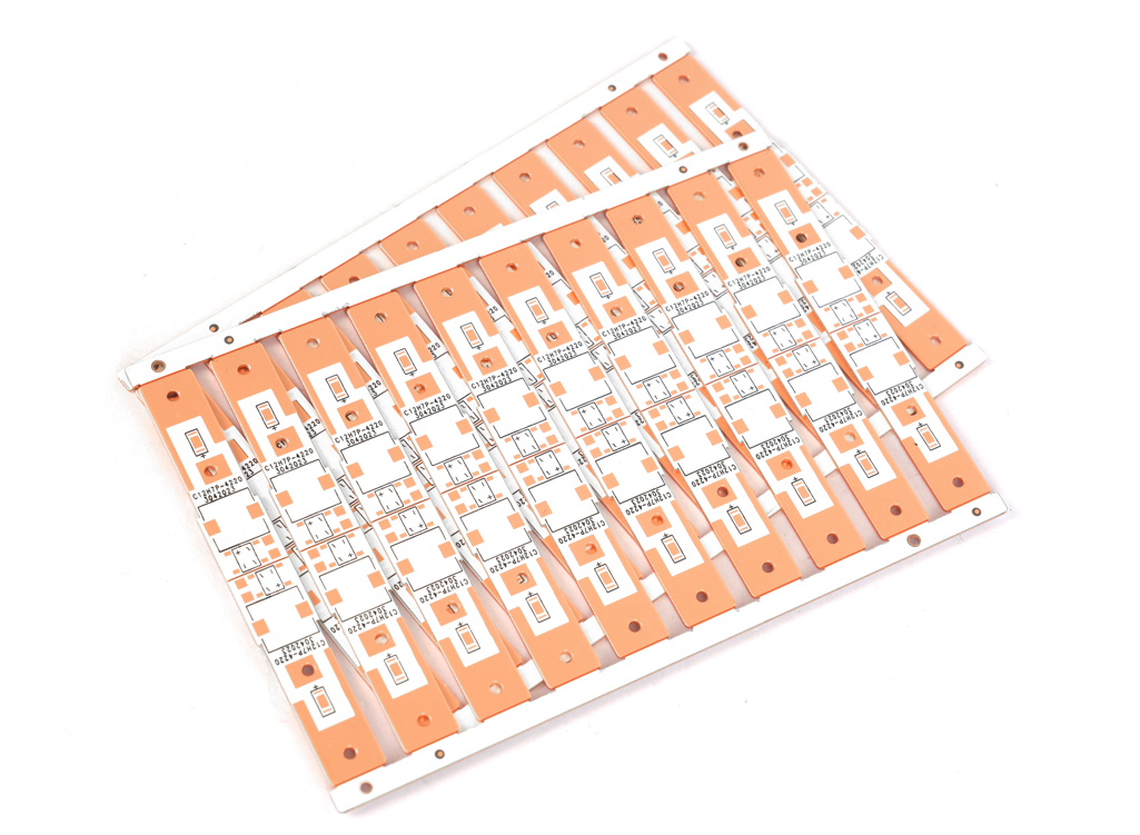
What is Bare Copper PCB?
A Copper PCB naked is a circuit board that is not coated where the raw copper layer remains completely exposed. Pursued from traditional surfaces such as gold or lead coating, this design maximizes the inherent nature of copper, extraordinary conductivity (5.9ane – 10 · S/M) and thermal dissipation (400W/Mâ · K). Ideal for high frequency applications such as 5G and Power Electronics, it offers cost savings (15-20%reduction) while maintaining signal integrity by eliminating signal loss induced by coating.
What are the benefits of an empty copper PCB?
- Cost efficiency – There is no additional surface layer (for example, Enig, Hasl) reduces production costs by up to 15â € “30%.
- Superior conductivity -The pure institution provides low resistance, ideal for high -speed signals and low loss transmission.
- Improvement of thermal performance -Natural Copper Thermal Conductivity (385 W/Mâ · K) efficiently eliminates heat in high power applications.
- Design flexibility – Untreated surfaces allow easy modifications (for example, etching, solder) during prototypes or customization.
- Environmental compliance – Avoiding chemical coatings, reducing dangerous waste and parallel to the Rohs/reach standards.
- Fast prototype – The simplified production process shortens the waiting time for testing and recurring design.
- Mechanical power – Thick copper layer (for example, 2oz/70î¼m) resistant to the arch and physical pressure in a rough environment.
What is an empty copper PCB board application?
- Fast Prototype & Iteration: Analyst costs for circuit design testing before completing surface finishing.
- High power electronics: Used in power supply, motor control, and LED driver for efficient heat dissipation.
- RF/Microwave Circuit: Ideal for antenna, filter, and amplifier due to low signal loss from pure copper.
- DIY Custom Project: Flexible for fans to modify traces, solder components, or experiment with layout.
- Thermal management system: Integrated into the heat sink, LED backlight, or high -current connector.
- Educational & Training Tools: Teach the basis of PCB, solder, and circuit design without complex coatings.
- Environmentally friendly device: Set products that are in accordance with Rohs that avoid chemical layers (for example, medical devices).
Copper Bare PCB Design Guide
1. Selection of material
- Substrate: FR4 (General-Purpose), Polyimide (Temperature/Flexible), Aluminum Substrate (High-later).
- Copper thickness: 0.5oz (17î¼m) up to 3oz (105îlen), adjusted to the current requirements (2oz supports ~ 2a/mm).
2. Stackup layer
- The recommended 4-lapi structure: Layers of signals of soil-processed signal power, ensuring the impedance pathway is low.
- Land Aircraft Priority: Establish a special land aircraft in the inner layer; Minimize the signal loop area.
3. Thermal management
- Copper layout: Use a wide copper footprint (‰ ¥ 1.5mm wide) for a high current zone; Leverage Thermal Copper Conductivity (385 W/Mâ · K).
- VIAS Thermal: Add thermal Vias (0.3mm diameter, 30îiefm coating) to connect copper layers and eliminate heat.
4. ESD Protection
- Foundation: Includes critical areas with land aircraft; Connect the connector shell to the isolated soil pads through short traces.
- Protection device: Place the TV diode (‰ ¥ 15kv) near the I/O port; Save TV-TO-GRUND paths ‰2MM.
- Layout Isolation: Keep sensitive components (for example, CMOS IC) far from the edge of the board; Use a copper ring for protector.
5. Manufacturing & Compliance
- Copper thickness tolerance: ETSA accuracy control (± 10%) to avoid impedance deviations.
- Rohs Compliance: Prohibit tin/mercury; Use halogen -free substrate.
6. Signal & Power Design
- Signal trail: High -speed signal routes adjacent to the land field; Match the differential pair impedance (90â € “100î ©).
- Power Distribution: Use a wide copper footprint (‰ ¥ 2mm) to decrease low voltage; Place the decoupling capacitor (0.1îlen) near the electric pin.
7. Testing & Validation
- ESD testing: Meet the IEC Standard 61000-4-2 (call 8KV, 15KV water).
- Thermal Simulation: Validation of an increase in high -current temperature (target ‰ 10 ° C).
Naked Copper PCB Design Specifications
| Category | Specification |
| Final surface | Naked copper that is not coated (oxidation prevention is recommended) |
| Electricity | Conductivity: 5.9ane – 10 · S/M Current capacity: 30% higher than the coated trail |
| Hot | Thermal conductivity: 400W/mâ · k max operation temp: 150 ° C (continuous) |
| Design rules | Min Trace Width: 6MIL (0.15mm) Min Hole Size: 0.25mm |
| Layer option | Only one side/two sides (multilayer requires special processing) |
| Signal integrity | The skin effect is optimized for RF application> 10GHz |
| Manufacturing | Requires: -The bore process is not direct-bonded copper |
The process of making an empty copper pcb
1. Design & Layout: Produce the Gerber file with a width of copper, distance, and stackup layer (single/two sides or multilayer).
2. Material preparation: Cut the substrate (FR4, Polyimide, or Aluminum) to the board size. Apply adhesive to the multilayer board.
3. Drilling: Use CNC to drill/component holes. Tolerance: ± 0.05mm.
4. Coating through a hole: Copper electropplation into a hole (thickness: 15â € “25îief) to connect the layer.
5. Outer layer imaging: Cover with photoresist, describe to UV through a mask of art, develop to determine traces.
6. ETSA: Remove unprotected copper using alkaline etchant (for example, ammonium persulfate).
7. Solder Mask (Optional): Apply a liquid soldering mask that can be understood, described, and develop to protect copper.
8. Testing: Electricity Test (Probe/Fixture Flying) for shorts/opens. AOI Inspection for Traces Integrity.
9. Routing & V-Score: The board pieces to the final dimension using a CNC router.
10. Packaging: Vacuum seal boards with drying to prevent oxidation.
How do I choose an empty copper PCB manufacturer?
Methods about how to choose a naked copper pcb manufacturer:
Verification of Technical Ability: Layer thickness & copper
- Confirm support for multi-layer boards (for example, 12 € “40 layers) and thick copper (‰ ¥ 2oz/70old). Check the minimum/distance trail width (eg.
Certification & Compliance
- Prioritizing producers with ISO 9001 (quality), UL (safety), IATF 16949 (Automotive), and Rohs Certification (Environment). Ensure compliance with IPC-6012 (rigid PCB performance) and MIL-P-P-13949G (military/aerospace) if it applies.
Production capacity & delivery
- Prototyping speed: Find a prototype 24 hours or faster for urgent projects.
- Scalability: Make sure the capacity for mass production (for example, some automatic production lines).
Quality control
- Testing: Requires electricity testing (probe/flight fixture) and AOI inspection for defects detection.
- Control Material: Verification of copper thickness tolerance (± 10%) and substrate quality (FR4/Polyimide).
Industrial experience
- Choose producers with proven expertise in your sector (for example, automotive, medical, or high -speed design). Review case studies or client testimonials for validation.
Cost & Supply Chain
- Compare prices for small/medium batch. Choose producers with production that can be discredited to reduce costs per unit. Consider geographical closeness to minimize logistics costs.
Communication & Support
- Assessing responsiveness to technical questions and post-sales services. Ensure clear warranty requirements and defects resolution processes.
Step by step selection process
- Determine Requirements: Determine the number of layers, the thickness of copper, shipping schedule, and certification.
- Short List candidates: Use an industrial directory or trading platform to filter based on ability.
- Quote & sample request: Provide design files for cost estimates and evaluation of test samples.
- Audit Factory: Check equipment (for example, automatic coating paths) and quality control processes.
- Pilot Orders: Place small orders to validate quality and shipping reliability.
- Finalization of Partnership: Negotiate contracts with producers who meet all criteria.
How do you get an offer for a copper PCB project?
Documents required for quotations:
1. Design file
- Send the Gerber file (RS-274X format) with a stackup layer, copper trail, and drill data.
- Include a bomb (bill of material) if the component is pre-source.
2. Technical Specifications
- Board details: Dimensions, layers (single/double/multilayer), copper thickness (0.5ozâ € “3oz).
- Material: FR4, polymide, or aluminum substrate.
- Surface finishing: Determine the copper or optional naked (Enig, Hasl) coating.
3. Quantity & Time Limit
- Provide order volume (prototype, small batch, or mass production).
- Clarification of delivery time lines (urgent orders can be charged priority).
4. Special Requirements
- Highlight ESD protection, thermal through density, or compliance standards (Rohs, UL).
Why choose the best technology?
- Skill: 19+ years on a copper PCB, supporting a 40 -layer board and 6oz thick copper.
- Speed: 2 hours quote response and 24 hour prototype.
- Quality: Full IPC-6012 compliance and AOI/Electricity Testing.
Contact us now if you have a request for a metal core PCB: [email protected].
Tag: PCB copper bare, empty copper pcb board
This entry was posted on Friday, August 1, 2025 at 18:54 and submitted under the best PCB, BestTPCB, MCPCB, PCB Core Metal. You can follow any response to this entry through RSS 2.0 bait. You can leave a response, or trackback from your own site.
Game Center
Game News
Review Film
Berita Olahraga
Lowongan Kerja
Berita Terkini
Berita Terbaru
Berita Teknologi
Seputar Teknologi
Berita Politik
Resep Masakan
Pendidikan
Berita Terkini
Berita Terkini
Berita Terkini
review anime
Gaming Center
Originally posted 2025-08-01 17:30:09.