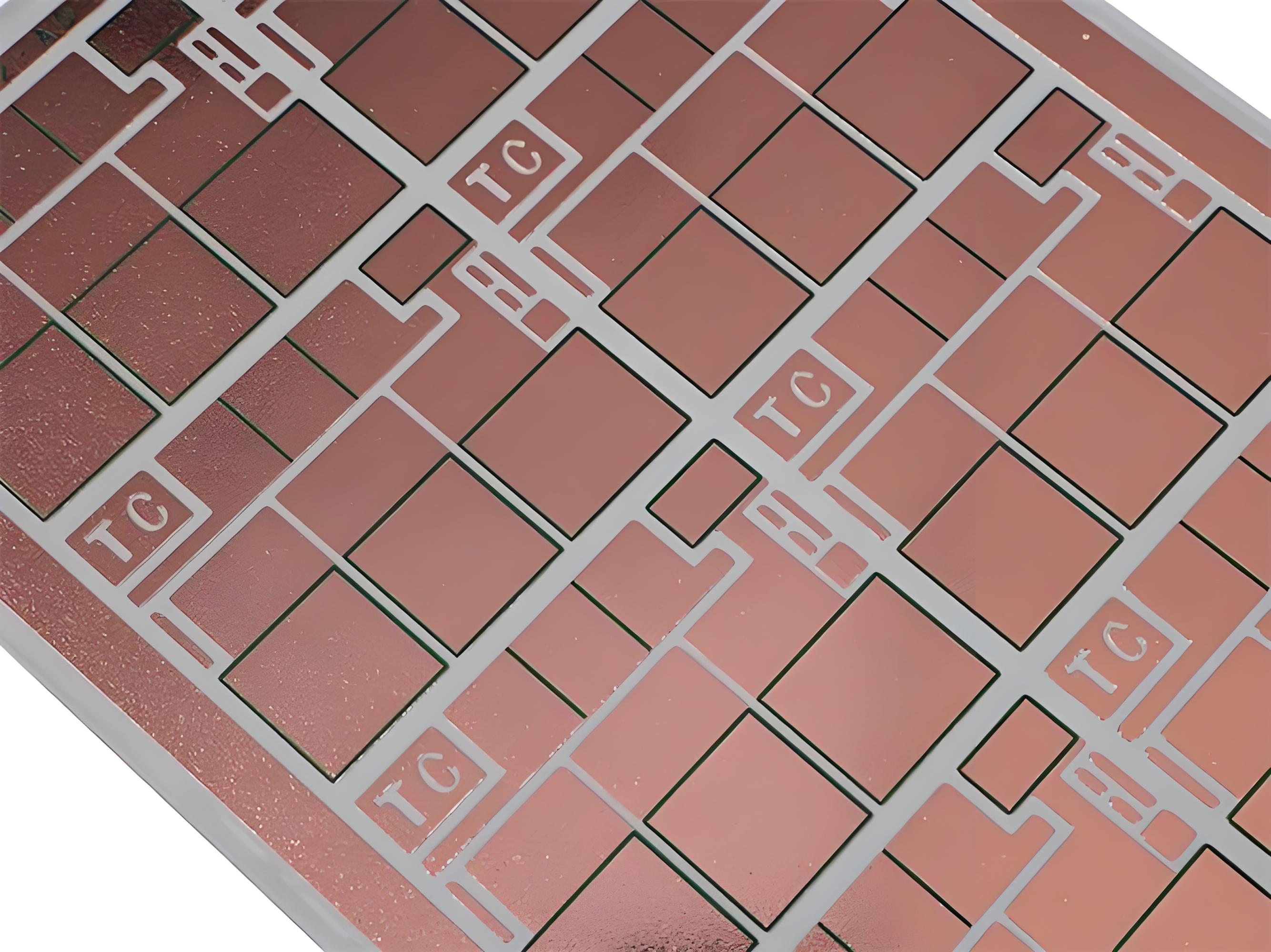
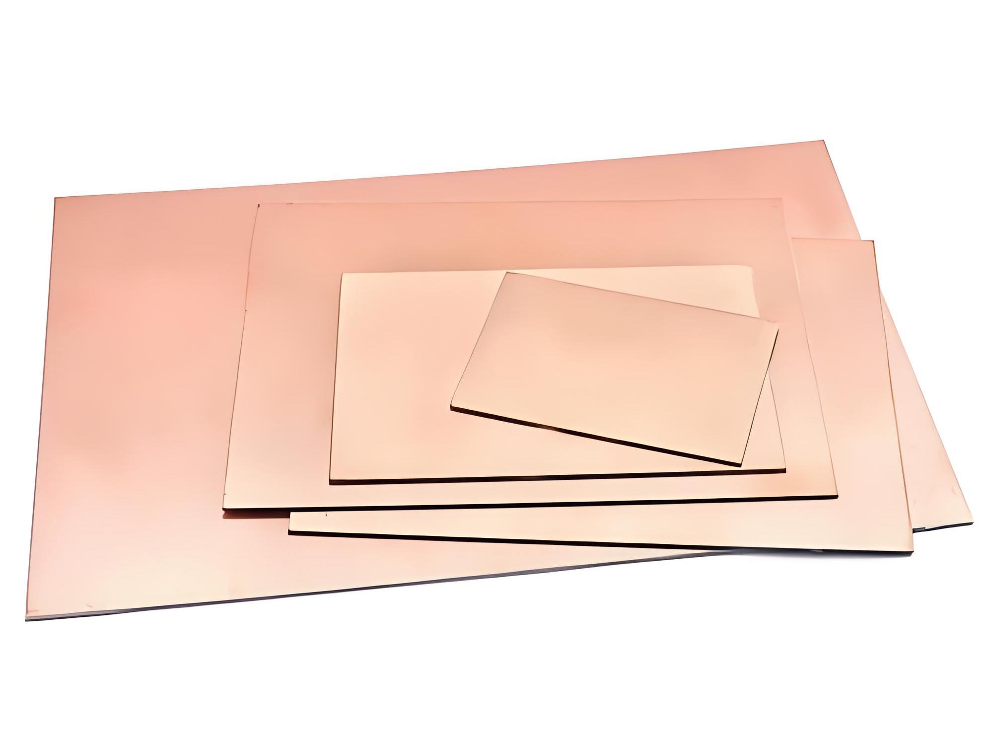
Copper PCB Clad is a core material for the print circuit board (PCB). Consists of insulation substrates and copper foil, these materials are pressed heat to form composites. Both support components and provide conductive circuits. Depending on the substrate, these materials can be categorized as paper, fiberglass, composite, or metal. They are widely used in consumer electronics, communication, automotive, and industrial control applications.
Do you want to know about the best PCBS Clad Copper Technology?
- Does the isolation performance meets circuit isolation requirements?
- Can the material strength hold the process of processing and use?
- Is the performance and balance balanced?
- Does the best technology provide customization and after -sales support?
The best copper PCB Clad can answer these questions.
- Compatible. Supports standard sizes and special specifications (thickness, shape), adapting to different PCB design requirements, and allows fast responses to small batch.
- Show. The basic ingredients are very resistant to bending and impact, and can withstand cutting, drilling, and other processing processes, preventing cracks or deformation after long -term use.
- Achieved. Performance meets industrial standards, with more than 100 council options for cost optimization, balancing reliability and affordability.
- Provide. Supports customization of materials, specifications, and processes. After sales service includes fast responses and warranty services, and accelerated orders are sent within 24 hours.
What is wrapped in copper on the PCB?
PCB wrapped in copper refers to the board where the thin layer of copper foil is bound to one or both sides of the substrate, usually fiberglass or other insulation material. This copper layer forms a conductive surface where the circuit pattern is then carved.
Without this copper clay, PCB will only be an insulator without the ability to carry a signal. With copper laminate to the substrate, the board gets electrical conductivity and becomes a foundation for electronic circuits.
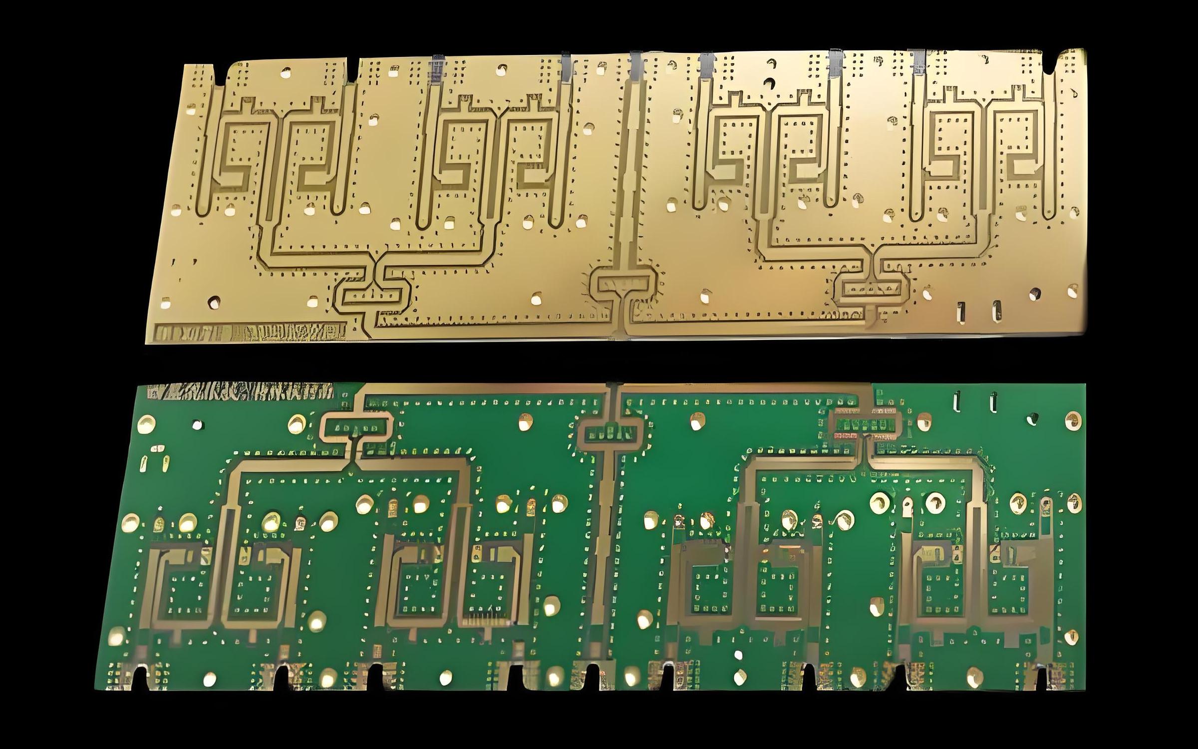
The copper clad board is then processed through techniques such as imaging, etching, and drilling to make pathways that allow electricity to flow between components.
In short, copper PCB boards are the starting point for almost every PCB. This bridges the gap between insulation material and conductive pathways.
How thick is the copper PCB dressing?
Copper thickness is one of the most critical specifications in the copper PCB clad sheet. This directly affects the current carrier capacity, heat dissipation, and endurance.
The thickness of copper in PCB is usually measured in ONS per square foot (OZ/ft²). This is what is usually seen:
- Copper 0.5 oz/ft² → about 18 thick microns
- 1 ounce/ft² copper → about 35 thick microns
- 2 ounces/ft² copper → about 70 thick microns
- 3 ounces/ft² and above → heavy copper, often used for electronic power
Standard consumer electronics often use 1 oz copper. High power applications may require 2 ounces or more to handle higher currents without overheating.
So, when choosing A Copper PCB Clad BoardThickness depends on the needs of your circuit and performance needs.
What is the laminated material layered copper (CCL)?
That Copper Clad Laminate (CCL) Not just copper. This is a combined material made of several layers. Each has a certain role.
Here are the main ingredients used:
1. Copper foil
- Conductive layer
- Provides paths for the current flow
- Usually treated to increase adhesion
2. Resin System
- Often modified epoxy or epoxy
- Acting as a binder
- Provide mechanical strength
3. Strengthening material
- Fiberglass fabric is the most common
- Ensure dimensional stability
- Increasing heat resistance
4. Additives
- Retardants API
- Filler for mechanical stability
- Special compounds for high frequency applications
This combination of elements gives copper dressed in pcb laminated Strong insulation, mechanical toughness, and long -term reliability.
Is that a PCB with copper wrapped only one side called?
PCB with laminated copper only on one side is known as a copper -dressed one -sided board. This is the simplest form of a PCB copper -coated laminate.
This is widely used on low -cost electronic devices and less complex. For example:
On the other hand, the two -sided copper PCB Clad board has a copper foil on both sides. This allows a more complex design and higher component density.
Therefore, depending on the complexity of the circuit, the one -sided or two -sided option can be selected.
What is the type of Copper Clad Lamination (CCL)?
Copper clad lamination Available in various types that match various applications. Here are the main categories:
Based on the substrate
- Paper -based (phenolic resin) → Affordable, good for household appliances
- Glass cloth (epoxy resin) → more durable, widely used in general electronics
- CCL composite → Paper and fiberglass mixture
Based on copper foil
- Electrolytic copper foil → smooth surface, ideal for precision circuits
- Copper foil rolled → excellent tenacity, used in a flexible PCB
Based on the application
- CCL General Purpose → cost -effective and widely used
- CCL high frequency → Designed for RF and Microwave devices
- High -speed CCL → used in data communication systems
- Thermal conductive CCL → Good for LED and Power devices
Each type of Copper Clad laminated PCB material is designed to handle unique performance demands.
Why use a copper PCB board?
Copper Clad PCB brings several advantages that make it the preferred choice:
- Very good conductivity: Copper provides a stable and reliable current flow.
- Thermal Management: Thicker copper spreads heat efficiently, prevent damage.
- Mechanical strength: Fiberglass strengthening increases stability.
- Design flexibility: Available in a single, double, or multilayer form.
- Cost efficiency: Paper -based and FR4 Lamination reduces production costs.
These advantages have caused the use of the PCB Clad Copper widely in consumer electronics, automotive systems, and medical devices.
What is the copper used for?
Copper clad boards function as a basis for many electronic products. Some main applications include:
1. Consumer Electronics
- Smartphone, tablet, laptop
- Device that can be worn
2. Automotive electronics
- Control module
- Safety system
- Infotainment unit
3. LED lighting
- High thermal conductivity version
- Used in aluminum substrate LED lighting
4. Industrial Control System
- Strong design for high currents
- Suitable for a hard environment
5. Medical device
- Concise and reliable circuit
- Long -term performance stability
In short, a copper PCBS Clad is needed wherever a reliable electronic connection.
How do I choose a copper dressed board for PCB?
Choosing the right Clad Clad Lamination PCB requires the performance of balancing, cost, and application needs. Here’s the way you decide:
1. Power requirements
- High current? Choose thicker copper.
- Low power? Standard copper 1 oz is enough.
2. Frequency performance
- For RF circuits or high -speed, select low loss lamination.
- For simple circuits, FR4 is cost effective.
3. Thermal demands
- LEDs and power devices benefit from thermal conductive laminate.
4. Design complexity
- One side for a simple device.
- Two sides or multilayer for complex design.
5. Budget Considerations
- Paper -based lamination is cheaper.
- Lamination of glass fiber offers a longer life.
By considering these factors, you can choose the best Copper clad board pcb For your project.
On Best TechnologyWe specialize Laminated Laminated PCB Copper It meets international standards and provides long -term reliability. If you are looking for a trusted supplier for your Copper Copper PCB board, our team is here to help. Contact us today at [email protected]
Tags: Copper clad laminated PCB, copper clad PCB, copper clad PCB board, copper PCB clad material, PCB copper -coated board, PCB copper laminated laminated
This entry was posted on Thursday, August 21, 2025 at 10:53 am and was submitted under the FAQ, FR4 PCB, PCB Technology. You can follow any response to this entry through RSS 2.0 bait. You can jump to the end and leave a response. Pinging is currently not permitted.
Game Center
Game News
Review Film
Berita Olahraga
Lowongan Kerja
Berita Terkini
Berita Terbaru
Berita Teknologi
Seputar Teknologi
Berita Politik
Resep Masakan
Pendidikan
Berita Terkini
Berita Terkini
Berita Terkini
review anime
Gaming Center
Originally posted 2025-08-21 07:54:53.