Through hole circuit board is a printed circuit board designed with drilled holes that allow component leads to pass through the PCB and be soldered on the opposite side. This article explains through hole components, plated through holes, through hole PCB assembly, soldering methods, SMT comparison, and key checks before ordering a through hole PCB.
Although surface mount technology is now widely used in compact electronics, through hole technology is still important. Many engineers choose it when a circuit needs stronger mechanical support, easier manual assembly, higher repairability, or reliable mounting for connectors, switches, terminals, relays, transformers, and other larger components.
If you are comparing PCB assembly options, the question is not simply “Is through hole old or new?” A better question is: Does the application need the mechanical strength, assembly flexibility, or component style that through hole design provides?
What Is a Through Hole Circuit Board?
A through hole circuit board is a PCB with drilled holes for component leads. The leads go through the board and are soldered to pads on the other side. This structure creates both an electrical connection and a mechanical anchor.
In many PCB drawings, through hole technology may also be called:
- Through hole PCB
- Through hole printed circuit board
- THT PCB
- Through hole circuit board
- Plated through hole circuit board
- Through-hole circuit board assembly
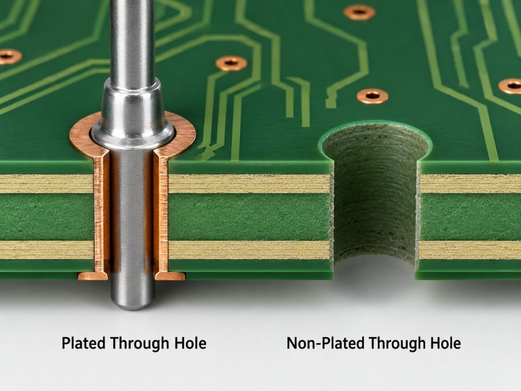
The basic structure is simple. The PCB has copper pads around the holes. In a plated through hole, copper is deposited on the hole wall. This copper connects the top layer, bottom layer, and sometimes inner layers in a multi-layer PCB.
A through hole circuit board may use two main hole types:
- Plated through holes
These holes have copper plating inside the hole wall. They are used for electrical connection between layers and for component soldering. - Non-plated through holes
These holes do not have copper inside. They are often used for mechanical mounting, screws, tooling, or positioning.
Through hole circuit boards are still common in industrial control, automotive electronics, power supplies, audio products, aerospace electronics, LED systems, test equipment, and many electronic devices that need durable solder joints.
The main value of through hole design is strength. Component leads pass through the board, so the solder joint is not only on the surface. This is useful for components that may face mechanical stress, vibration, frequent plugging, or heavier weight.
What Are Through Hole Components?
Through hole components are electronic parts with metal leads that pass through holes in a PCB. After insertion, the leads are soldered to copper pads on the opposite side of the board.
If a user asks “what are through hole components circuit boards,” they are usually trying to understand the relationship between the component and the board. The answer is straightforward: through hole components need holes in the circuit board so their leads can be inserted and soldered.
Common through hole components include:
- Resistors
- Capacitors
- Diodes
- LEDs
- Transistors
- IC sockets
- Pin headers
- Connectors
- Terminal blocks
- Relays
- Switches
- Transformers
- Inductors
- Fuses
- Battery holders
Through hole components are often larger than surface mount components. They are easier to hold, insert, solder, inspect, and replace. This is one reason they are still popular in prototypes, educational boards, repairable products, and low-to-medium volume industrial projects.
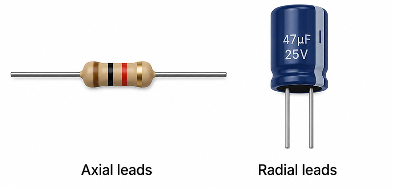
Through hole components usually come in two lead styles:
- Axial leads
The leads come out from both ends of the component body. Many traditional resistors and diodes use this style. - Radial leads
The leads come out from the same side of the component body. Many capacitors, LEDs, relays, and connectors use this style.
Through hole components are useful when the component must stay firmly attached to the PCB. For example, a power connector or terminal block may experience pulling force during wiring. A through hole design can help the board handle this stress better than a surface-only solder joint.
However, through hole components also take more board space. They require drilled holes, and the holes may reduce routing space on inner layers. For this reason, many modern designs use a mixed assembly approach: SMT for small parts and through hole for mechanically stressed parts.
What Is a Plated Through Hole?
A plated through hole, often called PTH, is a drilled hole with copper plating on the inner wall. This copper creates an electrical path between PCB layers. It can also support the soldering of through hole component leads.
A plated through hole is one of the most important structures in a through hole printed circuit board.
It can serve several functions:
- Connect the top layer to the bottom layer
- Connect outer layers to inner layers in multilayer PCBs
- Hold through hole component leads
- Improve mechanical bonding between component and board
- Support current flow through the PCB
- Provide a solderable barrel for component assembly
The manufacturing process usually includes drilling, hole cleaning, electroless copper deposition, and copper electroplating. The goal is to build a continuous copper layer inside the hole wall.
The quality of printed circuit board through hole plating matters because weak hole-wall copper can cause reliability problems. Common risks include:
- Thin copper plating
- Barrel cracks
- Voids in the hole wall
- Poor copper adhesion
- Resin smear
- Incomplete cleaning after drilling
- Poor solder filling during assembly
For reliable products, PTH quality should be checked during PCB manufacturing. In many industrial and high-reliability applications, manufacturers may use inspection methods such as microsection analysis, electrical testing, solderability testing, and visual inspection.
A plated through hole is not just a hole. It is an engineered interconnection structure. If the hole wall plating is poor, the board may pass visual inspection but fail later under thermal stress, vibration, or repeated operation.
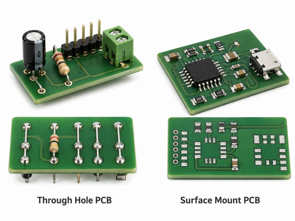
Through Hole PCB vs Surface Mount PCB
Through hole PCB and surface mount PCB are two different assembly approaches. Through hole technology uses component leads inserted through drilled holes. Surface mount technology uses components soldered directly onto pads on the PCB surface.
Most modern electronic products use SMT because it supports compact size, high assembly speed, and high component density. However, through hole technology still has strong value in specific applications.
Here is a simple comparison:
| Item | Through Hole PCB | Surface Mount PCB |
|---|---|---|
| Component Mounting | Leads pass through holes | Components sit on surface pads |
| Mechanical Strength | Stronger for large parts | Good for small/light parts |
| Assembly Speed | Slower | Faster |
| Board Density | Lower | Higher |
| Manual Soldering | Easier | More difficult for small parts |
| Repairability | Easier | Depends on package |
| Best For | Connectors, relays, terminals, power parts | Compact electronics, ICs, passive parts |
Through hole design is often better for:
- Large connectors
- Mechanical switches
- Terminal blocks
- Relays
- Transformers
- High-power components
- Test points
- Components exposed to stress
- Prototypes and repairable boards
SMT is often better for:
- Small consumer electronics
- High-density PCB layouts
- Automated mass production
- Fine-pitch IC packages
- Compact modules
- High-speed assembly
Many PCB assemblies use both. This is called mixed technology assembly. In this approach, small resistors, capacitors, ICs, and signal components use SMT, while connectors, power parts, and mechanical parts use through hole.
This is often the best balance. SMT saves space and cost, while through hole improves strength where it is needed.
When Should You Use a Through Hole Circuit Board?
You should use a through hole circuit board when the design needs stronger mechanical support, easy replacement, reliable manual assembly, or components that are not suitable for SMT.
Through hole technology is especially useful when the component will face movement, force, vibration, or frequent connection and disconnection.
Common use cases include:
- Connectors and terminal blocks
These parts may experience pulling force during wiring or use. - Power components
Large capacitors, inductors, transformers, and relays often need strong mounting. - Industrial control boards
Through hole parts are useful in rugged equipment and control systems. - Automotive electronics
Some parts need stronger joints due to vibration and temperature change. - Aerospace and defense electronics
High-reliability applications may use through hole parts where mechanical strength matters. - Prototypes and test boards
Through hole components are easier to solder, modify, and replace. - Repairable products
A through hole part is often easier to remove and replace than a tiny surface mount package.
Through hole circuit boards are not always the smallest or cheapest option. They require drilling, component insertion, and sometimes wave soldering or selective soldering. But they can provide a better choice when reliability, assembly flexibility, or mechanical strength matters more than extreme miniaturization.
A practical rule is simple: use SMT where density and speed matter, and use through hole where strength, serviceability, or component style matters.
How Is a Through Hole Circuit Board Made?
A through hole circuit board is made through a PCB fabrication process that includes material preparation, drilling, plating, imaging, etching, solder mask, surface finish, and final inspection.
The exact process depends on the board layer count, material, hole size, copper thickness, tolerance, surface finish, and application requirements.
A typical process includes:
- Material preparation
The manufacturer selects the laminate, copper thickness, and stack-up. - Drilling
Mechanical drilling creates through holes, mounting holes, and via holes. - Deburring and cleaning
The holes are cleaned to remove drilling debris and resin smear. - Electroless copper
A thin copper layer is deposited inside the holes to make the hole wall conductive. - Copper electroplating
Additional copper is plated on the hole wall and board surface. - Image transfer and etching
Circuit patterns are formed by photo imaging and copper etching. - Solder mask application
Solder mask protects copper areas and defines soldering pads. - Surface finish
Common finishes include HASL, ENIG, OSP, immersion tin, and immersion silver. - Routing and profiling
The board outline, slots, and cutouts are formed. - Electrical test and inspection
The finished board is tested for opens, shorts, dimensions, and workmanship.
Through hole reliability depends heavily on drilling and plating quality. If the hole is not clean, or if the copper plating is not consistent, the connection may become weak. This is why plated through hole quality control is important for industrial and high-reliability PCBs.
For multilayer boards, through hole plating is even more important because one plated hole may connect several layers. A defect inside the hole wall can affect the whole circuit.
What Is Through Hole Circuit Board Assembly?
Through hole circuit board assembly is the process of inserting through hole components into the PCB and soldering them to form electrical and mechanical connections.
The process may be manual, semi-automatic, or automated, depending on quantity, component type, and project requirements.
A typical through hole circuit board assembly process includes:
- Component preparation
Components are checked, counted, formed, or cut if needed. - Component insertion
Leads are inserted into the correct holes according to the assembly drawing and BOM. - Pre-solder inspection
Operators check component position, polarity, height, and orientation. - Soldering
The board may be soldered by wave soldering, selective soldering, or hand soldering. - Lead trimming
Extra lead length may be trimmed after soldering. - Cleaning
Flux residue may be cleaned depending on flux type and product requirements. - Inspection
Solder joints are checked for filling, wetting, bridges, insufficient solder, and other defects. - Testing
The assembled board may go through ICT, functional testing, programming, or final inspection.
Common soldering methods include:
- Wave soldering
Efficient for boards with many through hole components. - Selective soldering
Useful when the board also has SMT components that must avoid wave solder exposure. - Hand soldering
Common for prototypes, small batches, repair, and special components.
Through hole circuit board assembly is often used in products where mechanical strength and component durability matter. It is also common in mixed assembly projects, where SMT and through hole components are assembled on the same board.
For buyers, the important point is to provide complete assembly files. These usually include Gerber files, BOM, pick-and-place file if SMT is included, assembly drawing, polarity markings, test requirements, and special soldering instructions.
How to Solder Through Hole Components?
Soldering through hole components requires clean pads, correct component placement, suitable solder temperature, proper solder flow, and good inspection. A strong solder joint should wet both the component lead and the PCB pad.
For basic manual soldering, the process is:
- Insert the component into the correct holes.
- Check polarity and orientation.
- Bend or hold the leads slightly if needed.
- Heat the pad and component lead at the same time.
- Feed solder into the joint, not directly onto the iron tip.
- Let the solder flow around the lead and pad.
- Remove solder first, then remove the iron.
- Let the joint cool naturally.
- Trim extra lead length if required.
- Inspect the solder joint.
A good through hole solder joint usually looks smooth, bright, and slightly concave. It should show proper wetting around the lead and pad.
Common through hole soldering defects include:
- Cold solder joint
- Insufficient solder
- Solder bridge
- Excess solder
- Poor wetting
- Lifted pad
- Cracked joint
- Unfilled barrel
- Wrong component orientation
- Burned pad or damaged solder mask
For production assembly, soldering quality should be checked according to the required workmanship standard. For industrial and high-reliability products, solder filling, cleanliness, lead length, component height, and polarity should be controlled carefully.
Through hole circuit board solder quality is not only about appearance. A poor solder joint may pass a quick visual check but fail later due to vibration, thermal cycling, or mechanical stress.
What Should You Check Before Ordering a Through Hole PCB?
Before ordering a through hole PCB, buyers should check both the PCB fabrication requirements and the assembly requirements. Many problems come from unclear files, missing tolerances, or incomplete component information.
A useful checklist includes:
- Gerber files
Confirm that the production files are complete and updated. - Drill files
Check hole size, plated holes, non-plated holes, slots, and tolerances. - Stack-up
Define layer count, board thickness, copper thickness, and material. - Hole plating requirements
Confirm plated through holes, hole-wall copper, and any reliability requirements. - Component lead diameter
Make sure hole size fits the component leads after plating. - Annular ring
Check pad size around the hole to avoid weak soldering or breakout risk. - Surface finish
Choose HASL, ENIG, OSP, immersion tin, or other finish based on assembly needs. - Soldering method
Confirm whether the project uses wave soldering, selective soldering, or hand soldering. - BOM and assembly drawing
Provide clear component references, polarity, part numbers, and placement notes. - Testing requirements
Define electrical test, AOI, functional test, ICT, or customer-specific inspection. - Quantity and delivery schedule
Prototype, small batch, and mass production may need different process planning. - Repair or service needs
If the product must be repaired in the field, through hole components may be helpful.
A good through hole PCB quote should not be based only on board size and quantity. Hole count, hole tolerance, plating quality, component insertion, soldering method, inspection level, and testing needs can all affect cost and lead time.
If the product has mixed SMT and through hole assembly, it is better to ask the manufacturer to review the full process before production. This helps prevent soldering conflicts, component height issues, masking problems, and rework risks.
FAQs About Through Hole Circuit Board
What Is a Through Hole Circuit Board?
A through hole circuit board is a PCB with drilled holes for component leads. The leads pass through the board and are soldered to pads on the other side.
What Are Through Hole Components?
Through hole components are electronic parts with leads that go through holes in a PCB. Common examples include resistors, capacitors, connectors, terminal blocks, switches, relays, transformers, and LEDs.
What Is a Plated Through Hole?
A plated through hole is a drilled hole with copper plating on the hole wall. It provides electrical connection between PCB layers and supports through hole component soldering.
Is a Through Hole PCB Better Than an SMT PCB?
Not always. Through hole PCB is better for mechanical strength, repairability, and large components. SMT PCB is better for compact size, high-density layout, and fast automated assembly.
Can Through Hole and SMT Be Used on the Same PCB?
Yes. Many PCB assemblies use both. SMT is used for small components, while through hole is used for connectors, terminals, relays, and other mechanically stressed parts.
Why Are Through Hole Components Still Used?
They are still used because they provide strong solder joints, easy handling, easier repair, and good reliability for large or stressed components.
What Is Through Hole Circuit Board Assembly?
Through hole circuit board assembly is the process of inserting through hole components into PCB holes and soldering them by wave soldering, selective soldering, or hand soldering.
How Do You Solder Through Hole Components?
Insert the component, heat the pad and lead, apply solder, allow it to flow properly, remove the solder and iron, let the joint cool, trim the leads, and inspect the joint.
Can a Through Hole Circuit Board Be Repaired?
Yes. Through hole boards are usually easier to repair than dense SMT boards. However, care is needed to avoid lifted pads, damaged plated holes, or broken traces.
What Files Are Needed for a Through Hole PCB Quote?
You should provide Gerber files, drill files, stack-up, BOM, assembly drawing, surface finish requirements, quantity, test requirements, and any special soldering notes.
In summary, through hole circuit board is still a practical choice when electronic products need strong component mounting, easy repair, stable solder joints, and reliable assembly for larger parts. It is especially useful for connectors, terminals, relays, power components, prototypes, industrial control boards, and mixed-technology PCB assemblies.
The key is to understand how through hole components, plated through holes, PCB drilling, hole plating, soldering, and inspection work together. A well-designed through hole PCB should not only fit the circuit schematic; it should also support reliable manufacturing and assembly.
If you need through hole PCB manufacturing, through hole PCB assembly service, DFM review, or mixed SMT and THT assembly support, send your Gerber files, BOM, stack-up, drawings, and project requirements to EBest Circuit (Best Technology) at [email protected].
Tags: Through Hole Circuit Board, through hole circuit boards, through hole printed circuit board
PakarPBN
A Private Blog Network (PBN) is a collection of websites that are controlled by a single individual or organization and used primarily to build backlinks to a “money site” in order to influence its ranking in search engines such as Google. The core idea behind a PBN is based on the importance of backlinks in Google’s ranking algorithm. Since Google views backlinks as signals of authority and trust, some website owners attempt to artificially create these signals through a controlled network of sites.
In a typical PBN setup, the owner acquires expired or aged domains that already have existing authority, backlinks, and history. These domains are rebuilt with new content and hosted separately, often using different IP addresses, hosting providers, themes, and ownership details to make them appear unrelated. Within the content published on these sites, links are strategically placed that point to the main website the owner wants to rank higher. By doing this, the owner attempts to pass link equity (also known as “link juice”) from the PBN sites to the target website.
The purpose of a PBN is to give the impression that the target website is naturally earning links from multiple independent sources. If done effectively, this can temporarily improve keyword rankings, increase organic visibility, and drive more traffic from search results.