When creating modern electronic devices, every important step-from the first sketch to the final product. If you explore the printing circuit board process, or PCB, this guide is a one -stop resource. and cost efficiency.
What is a printed circuit board?
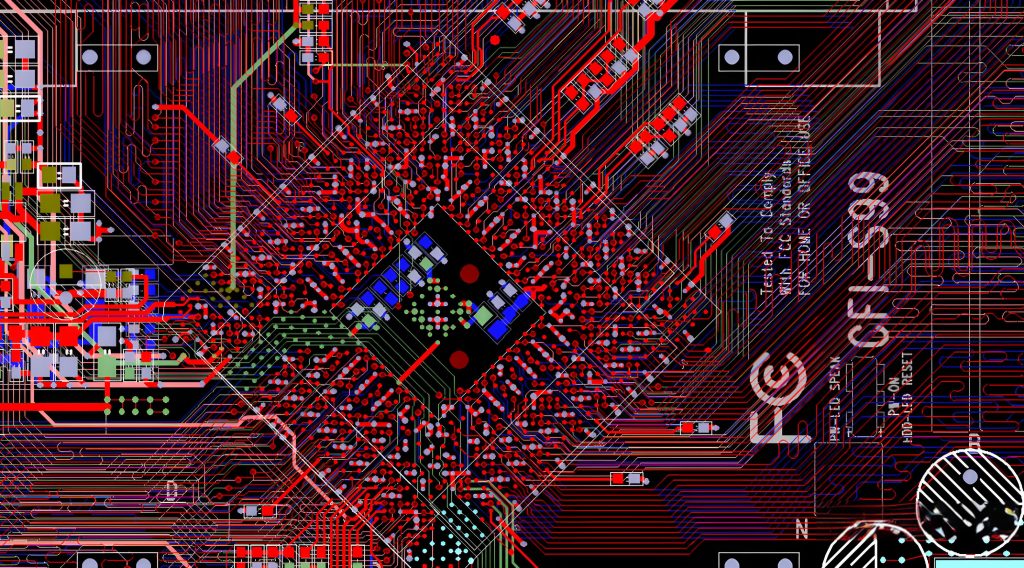
Print circuit board (PCB) is the backbone of almost all electronic systems. This flat SA board holds and connects electronic components using conductive tracks, pads, and VIAS is engraved from copper sheets that are laminated to non-conductive substrates. Common ingredients include FR4, ceramics, aluminum, and polymide.
PCB comes in various forms: PCB one side side, two sides, and multilayer, support everything, ranging from simple gadgets to complex military electronics. Their role is simple but critical: providing physical support and reliable electricity.
How to design a PCB board?
The PCB design phase regulates the tone for the entire life cycle. This starts by defining the scheme, which maps the electronic connection between the components. After that is ready, the designer moves to the layout – placing components and traces of the stomach.
Key steps include:
- Creating schemes using software such as altium designer, kicad, or eagle.
- Establish footprints to components for the right placement.
- Define the dimensions of the board, piles of layers, and signal flow.
- Stomach signals with attention to the width, impedance, and permission.
- Add VIAS, Pour Copper, and Power Plane for optimal performance.
- Check rules design (DRC) to verify distance, traces, and other obstacles.
- Produces Gerber files, which are manufacturing blueprints.
Each design must balance space, power, heat, cost, and manufacturing. One detail that is ignored can delay all your projects.
Consideration during the PCB design phase
Designers must turn many variables beyond schematic accuracy. The following are important considerations to optimize performance and reduce the risk of failure:
1. Placement of components: Keep the analog circuit, digital, and separate power to reduce interference. The group -related components are logically to minimize the length of the track.
2. Signal integrity: For high -speed design, impedance matching, a differential couple, and minimizing crosstalk is very important.
3. Thermal management: Use the thermal Vias, pour copper, and heat sink to handle heat dissipation, especially in power electronics.
4. Design for Production (DFM): Make sure the width of the trail, the size of the drill, and the free distance of the ability of the producer.
5. EMC and EMI Compliance: Fire, protector, and filtering components help meet the regulatory standards.
6. Mechanical Constraints: Do not face the installation hole, align the connector, or fit enclosure. This small detail can turn into an expensive mistake later.
A good design minimizes re -work, increases life, and lowering costs throughout production.
Complete PCB Fabrication Process – step by step
After the design is complete, the PCB fabrication process converts digital files into real boards. This is the way that occurs:
1. Selection of material
The manufacturer selects basic ingredients such as FR4, aluminum, or ceramics depending on thermal, mechanical, and electricity requirements.
2. Internal layer imaging (for Multilayer PCB)
Each layer of copper in patterned with circuits using phoresists, UV exposure, and ETSA techniques.
3. Lamination
The inner layer is engraved and laminated under the heat and pressure, forming a solid multilayer structure.
4. Drilling
The hole is drilled to make VIAS for electrical connections between layers. Laser drilling is used for microvias.
5. Plating and copper deposition
Coated holes with copper using electroplating to ensure conductivity in all layers.
6. Outer layer imaging
The outer copper layer is patterned similar to the inner layer using photoresist and etching.
7. Solder Mask Application
The solder mask is applied to isolate boards and protect traces, leave the bearing and open holes to solder.
8. printing silkscreen
Component labels, logos, and reference indicators are printed on the blackboard.
9. Surface is complete
Surfaces such as Hasl, Enig, OSP, or Silver Soaking are applied to copper bearings that are open to protect it and improve the ability of solder.
10. Electric testing
Probe flies or a bed test checks the circuit and open shorts.
General PCB assembly problems during manufacturing
During the PCB assembly, the component is installed and soldered to the board. This phase can be manual or automatically use SMT (Surface-Mount Technology) and ENT (technology through holes).
But some problems can interfere with this process:
1. Tombstoning: Components lifted on one side during reflow, causing connectivity failure.
2. Solder Bridge: Excessive solder connects two pins accidentally, which leads to a short circuit.
3. Cold connection: Poor solder produces weak mechanical bonds and unreliable connections.
4. Components that are not in harmony: Incorrect placement, often caused by poor paste applications or pick-and-plate calibration.
5. PCB warping: thin or large boards can bend during reflow, affect solder and mechanical integrity.
6. Damage components: heat or excessive treatment errors can destroy the ic or smooth capacitor.
Quality controls, professional assembly pathways, and well -prepared Gerber + Bomb files help avoid this problem.
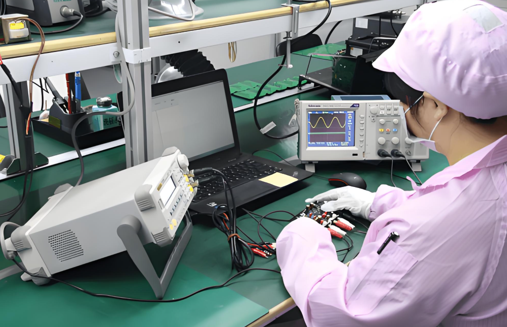
How to test the printed circuit board?
After the assembly, PCB testing ensures the product functions before the final integration. There are several levels of testing depending on the application and budget:
1. Visual inspection
The simplest method. Engineers check physical defects such as solder bridges, lost components, or alignment problems.
2. Automatic Optical Inspection (AOI)
AOI uses a camera to scan the board for the quality of solder, polarity, and the presence of components.
3. Circuit testing (ICT)
Test the electrical characteristics of each component by investigating specific test points. This is fast and accurate for large volume production.
4. Flying Probe Testing
Using Probot Robot to test low to medium volume PCB without the need for special equipment.
5. Functional Testing (FCT)
Verifying the complete PCB assembled in real world operating conditions. Important for high reliability applications.
Non -optional testing is very important. The wrong board costs, money, and customer trust.
Why consider the best Turnkey Technology service?
If you are tired of juggling several vendors for PCB design, fabrication, assembly, and testing, the best technology offers full Turnkey PCB services that simplify the process.
This is why clients around the world believe in us:
Technical Support Before & After Sales
 € Prototype & Speeches of Small Volume
 –an The Rext Out, Delivery on Time
 ž High quality, special demand is available
 € ž strong R&D team, know how to
 -U Rich Experience (> 13 years)
 ž Fast feedback (within 12 hours)
 ž One -stop service (PCBA/Assembly)
Conclusion
Print circuit boards are the heart of modern electronics, and get the correct design, fabrication, assembly, and testing cannot be negotiated. Each step has its roleâ € ”and skip or is in a hurry -any part of the part can cause expensive failure.
Whether you build a simple sensor or complex industrial controller, choosing partners like the best technology can make the trip more smoothly. We understand what is needed by engineers, startups, and procurement teams: fast delivery, quality control, and transparent communication.
FAQ
1. What software is used to design a PCB?
Tools such as altium designers, eagle, kicad, and ORCAD are generally used for schematic layout and PCB.
2. How long is the time for making a PCB?
Standard fabrication requires 3â € “7 days. Express services can provide within 24-48 hours depending on complexity.
3. What is the difference between PCB and PCBA?
PCB is a naked board. PCBA is a board after the component is assembled and soldered.
4. How much does the PCB assembly cost?
Costs vary based on the amount, complexity, type of section, and whether the parts are sourced by producers or supplied by the customer.
5. Does the best technology support low volume PCB manufacturing?
Yes. We support low and high volume production and offer prototype services for new design.
Tags: PCB assembly, PCB design, PCB fabrication, PCB testing, print circuit board
This entry was posted on Friday, June 6, 2025 at 17:36 and submitted under the best PCB, BestTPCB, FAQ, PCB News, PCB Technology. You can follow any response to this entry through RSS 2.0 bait. You can leave a response, or trackback from your own site.
Game Center
Game News
Review Film
Berita Olahraga
Lowongan Kerja
Berita Terkini
Berita Terbaru
Berita Teknologi
Seputar Teknologi
Berita Politik
Resep Masakan
Pendidikan
Berita Terkini
Berita Terkini
Berita Terkini
review anime
Gaming Center
Originally posted 2025-06-07 21:12:57.