Copper thickness is a key factor that affects the performance of your board. Choosing the right thickness of copper is an important part of the PCB design, it affects how well your circuit works, how long it takes place, and even how much it costs. On this blog, we will break down why the thickness of copper is important, how to choose the right option for your PCB design € ” – to help you make decisions based on information for your next project.
Why is the thickness of copper important?
1. Current front capacity
A thicker copper layer handles higher currents without too hot. For example:
- 1 Oz Copper: Supports up to ~ 3A per 10mm track width.
- 2 OZ Copper: Double capacity for ~ 6A for the same width.
- It is important for power circuits such as motor control or LED drivers.
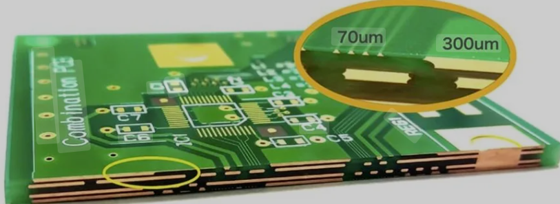
- 3 oz+ copper (140 µm+):
- Handles 12a+ per 10mm, suitable for extreme applications such as inverters or industrial power supplies. However, thicker copper increases fabrication costs and requires special manufacturing.
2. Signal integrity
High frequency design (for example, RF, 5G): thinner copper (0.5 ozâ € “1 ounce) with a smooth surface reduces signal loss.
Standard Circuit: 1 OZ Copper is enough for most low frequency applications.
3. Power
Thicker copper (‰ ¥ 2 oz) withstand the thermal voltage during the soldering and mechanical wear in a hard environment.
Thin copper (0.5 oz) can crack under repeated vibrations or changes in temperature.
4. Cost efficiency
Thicker copper increases material costs and requires longer ETSA time.
The thickness of excessive specifications wasting money; Poor risk failure.
How to choose the right thickness for your PCB?
Based on our 19+years of experience in the field of PCB manufacturing, today I want to share 6 strategies on how to choose the right thickness
1. Calculate the current requirements
Use standard tools or online IPC-215 (for example, Saturn PCB Toolkit) to determine the width of the minimum trail and the weight of copper for now.
Example: Power trail 5A with 1 oz copper requires 2mm wide. With 2 oz copper, width drops to 1mm, saving space.
2. Prioritize space vs. Performance
High density design: Use thinner copper (0.5 ozâ € “1 ounce) to match more traces.
Power-Heavy board: options for 2 oz ‘6 oz copper to reduce the width of traces and avoid excessive heat.
3. Factors within manufacturing limits
Thin copper (0.5 oz): vulnerable to over-ethching; requires tighter process control.
Thick copper (> 3 ounces): requires special coating and etching, increasing the waiting time and costs.
Common mistakes to avoid
- Ignoring current density: a thin trail with a high -current cause of fatigue.
- Excessive design: using 3 oz copper for low-power signals wasting space and money.
- Ignoring the manufacturer’s feedback: Always confirm the ability of your FAB House (for example, Max/min, copper weight).
Conclusion
Choosing the right thickness of copper balances performance, costs, and manufacturing. By aligning your design needs with industrial standards and the ability of producers, you can avoid expensive redesign and ensure long -term reliability.
Also, if you have more questions about the thickness of the PCB copper or need help with your design, don’t hesitate to contact the shipping question. We will help you optimize the thickness of copper and maximize the potential of your board.
Tags: PCB thickness, pcn design
This entry was posted on Saturday, June 7, 2025 at 9:50 am and was submitted under the best PCB, BestTPCB, FAQ, FR4 PCB. You can follow any response to this entry through RSS 2.0 bait. You can leave a response, or trackback from your own site.
Game Center
Game News
Review Film
Berita Olahraga
Lowongan Kerja
Berita Terkini
Berita Terbaru
Berita Teknologi
Seputar Teknologi
Berita Politik
Resep Masakan
Pendidikan
Berita Terkini
Berita Terkini
Berita Terkini
review anime
Gaming Center
Originally posted 2025-06-07 08:57:42.