At most technology, we offer SMT assembly and through holes for various types of PCBs. With ISO certification, our team guarantees the right quality and trace. Whether you are working on a PCB prototype or large volume order, we can handle a complete processâ € “from PCB fabrication to full assembly” with competitive prices and professional engineering support.
What is technology through a hole?
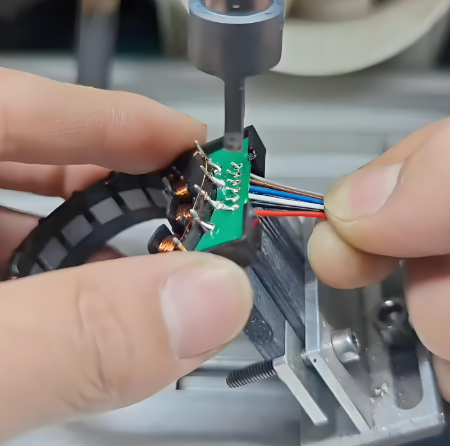
Through hole technology is a method used to install electronic components on the print circuit board (PCB). This involves drilling holes on the PCB where the component lead is inserted and soldered into the bearing on the opposite side. This process creates a strong mechanical bond, which is very useful for components that deal with higher currents or require more stability.
The term PCB through a hole refers to the space that is drilled where the lead passes and connects the circuit to a different layer. Although newer surface installation technology (SMT) is now more common, through holes are still widely used in specific applications such as aerospace, military, and the testing environment.
What are the characteristics of technology through holes?
Technology through holes has several decisive features that separate it from SMT. First, this requires the right drilling to the PCB, which can increase the time and production costs. Second, it uses the main component, which means the part has a metal cable that must be placed through a hole. Third, soldering can be done manually or with wave soldering, depending on the complexity and quantity of assembly.
Another key feature is the mechanical strength of the connection. Unlike the SMT component, parts through the hole have a deeper barrier, making it more reliable under pressure, vibrations, or high temperatures.
Various types of holes through
There are several types of PCBs through holes, each serving different purposes in the assembly process:
1. Layered through a hole (pth)
This is the most common. They have a conductive copper coating in the hole wall, creating an electric connection between the PCB layer. PTH is used for signal routing and installation components.
2. Non-Elephisies Through Hole (NPTH)
These holes do not have copper inside and are used pure for mechanical reasons such as installation screws or hardware. They do not connect circuits or carry currents.
3. Through the hole
Although often grouped separately, VIAS is also a type of hole through. They connect one layer of PCB to another electrically but not used to enter components. VIAS can be through VIAS, Vias Blind, or Vias buried depending on the layer they connect.
4. Component hole
This is specifically drilled for tin components such as resistors, capacitors, and connectors. They are usually PTHS because they need electrical connectivity and physical barriers.
What is the difference between SMT and technology through holes?
The main difference lies in how the components are installed to the PCB:
| Feature | Technology through holes | Mount Surface Technology (SMT) |
| Component placement | Lead is inserted through a drilled hole | Installed directly on the surface of the PCB |
| The side of the board is used | Both sides (top for components, bottom for solder) | Mostly one side |
| Type of assembly | Manual or soldering wave | Automatic Solder Reflow |
| Mechanical strength | Tall | Currently |
| Suitable for | High stress environment | Electronic with high density, lightweight |
| Cost | Higher due to drilling and manual labor | Lower with automatic production |
In short, technology through holes vs SMT often empties into reliability vs efficiency. SMT is ideal for modern and concise devices, while through a preferred hole for heavy or high reliability circuits.
What are the advantages through the hole?
- “Strong mechanical affair: through the hole gives a strong mechanical connection by welding the component pins to the PCB, suitable for holding a large mechanical voltage.
- â € œMature Process: The process of making holes through is relatively mature, at low costs, and is suitable for large scale production.
- “High compatibility: PCB through holes has good compatibility with component packaging forms, suitable for traditional packaging through holes and special-shaped components with larger size.
- For solder and manual maintenance: PCB through a comfortable hole for solder and manual maintenance, and can be completed with an ordinary soldering iron and other tools.
- Higher current capacity: larger leads and deeper soldering connections to handle more power.
- Reliable for prototypes: easier to work manually, which helps in R&D.
Disadvantage of technology through holes
Although useful in many cases, holes are also equipped with limitations:
- More expensive: drilling increases time and manufacturing costs.
- Lower component density: take more space on the PCB compared to SMT.
- Slower assembly: manual solder or waves are not as fast as SMT automatically.
- Two -sided processing: components on one side, solder on the other, re -work or inspection that is difficult.
- Affects signal integrity: In high -speed signal transmission, through a hole will produce parasitic capacitance and inductance, which can cause signal and crosstalk delay, affecting signal integrity.
These weaknesses make holes through high volume electronics or modern miniatures.
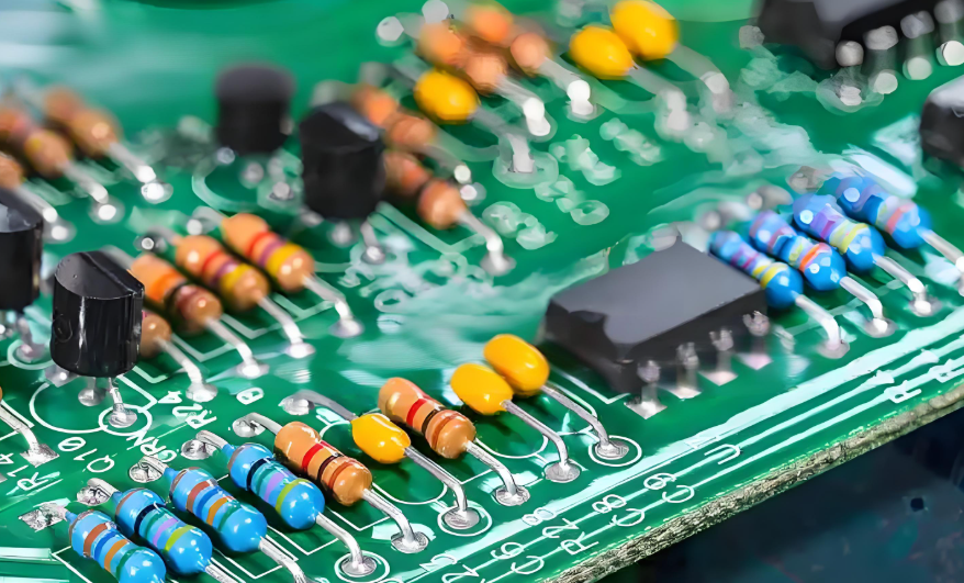
What material is used in hole technology?
The materials involved in assembly through holes include:
- PCB Substrate: Usually FR-4, Fiberglass material that is fireproof.
- Copper foil: used to jump over hole walls to make an electric connection.
- Solder: Generally tin or lead alternatives for Rohs compliance.
- Flux: helps the flow of solder and bonds to the metal surface.
- Main components: with metal leads or cables that pass through the board.
- Masking ink: protect areas that are not intended to solder.
These ingredients work together to create a strong and conductive connection that lasts from time to time.
Consideration during solder through the hole component
When soldering components through the hole, maintaining the following factors in the mind helps ensure a reliable and high-quality connection:
1. Matching hole size and lead
The drilled hole must match the tin diameter of the component. Too loose causing weak joints; Too tight limit the flow of solder.
2. The Right Solder Method
- Solder manual is ideal for a prototype or low volume assembly.
- Solder Wave matches a larger batch with consistent quality and speed.
3. Controlled Flux Application
Apply adequate flux to clean the surface and increase solder flow. Excess flux can leave residues or cause corrosion.
4. Accurate component placement
Lead must be inserted straight and fully into the hole to avoid stress during the soldering or newer use.
5. The correct temperature and time of the soldering
Maintain the right level of heat and remains time to prevent the soldering joints cold or too hot.
6. Avoid the soldering bridge
Make sure the solder does not accidentally connect two adjacent pads or tin, especially in strict areas.
7. Mechanical stability
For connectors or large components, use support equipment during solder to keep the spare parts from shifts.
8. Inspection after soldering
Check the smooth and shiny soldering joints. Use magnification or x-ray for solid or complex boards.
9. Post-solder cleaning
Remove residual flux residues with the right solvent or cleaning process to prevent long -term damage.
10. ESD safety steps
Handle components with ESD prevention measures to protect sensitive devices from electrostatic release during assembly.
What is the hole used for?
Through holes used in many fields of manufacturing and PCB assembly. Their main function is to:
- Install large components: such as capacitors, connectors, or inductors.
- Signal or transfer power: in some PCB layers.
- Anchor parts: where strong mechanical support is needed.
- Prototype Support: bread boards and experimental PCBs often use components through holes because it is easier to enter and replaced.
- Handle hard conditions: Ideal for products exposed to movement, heat, or the use of heavy tasks.
In short, PCB through hole design is a practical solution when strength, reliability, and improvement ability is the key.
FAQ
1. Is technology through the hole still used today?
Yes, especially in the application of aerospace, automotive, and high power where strength and reliability are very important.
2. Can through a hole and SMT is used on the same PCB?
Yes. Mixed technology boards combine the two methods to meet different design requirements.
3. Why is it better through a hole for testing?
The main component is more easily investigated and replaced, which helps during R&D or repairs.
4. Is through a hole more expensive than SMT?
In general, yesâ € ”due to manual labor, drilling holes, and larger component sizes.
5. Which is better: SMT or through a hole?
It depends. SMT is better for compact and automatic designs. Through holes are better for hard strength and environment.
Tag: through hole technology
This entry was posted on Monday, June 9, 2025 at 18:38 and submitted under the best PCB, BestTPCB, Design Guide, FAQ, PCBA, SMT Technology. You can follow any response to this entry through RSS 2.0 bait. You can leave a response, or trackback from your own site.
Game Center
Game News
Review Film
Berita Olahraga
Lowongan Kerja
Berita Terkini
Berita Terbaru
Berita Teknologi
Seputar Teknologi
Berita Politik
Resep Masakan
Pendidikan
Berita Terkini
Berita Terkini
Berita Terkini
review anime
Gaming Center
Originally posted 2025-06-09 21:19:57.