Robotics PCBs determine whether the robot moves with precision or drifts under load, whether sensor data remains stable or is distorted by noise, and whether the system survives real-world vibrations and thermal cycles. In industrial robotics and AI-based platforms, PCB design and manufacturing discipline are often the deciding factor between scalable deployment and repeated field failures.
From the customer’s perspective, robotics projects often face structural obstacles during the transition from prototype to production:
- Motion instability under dynamic loads
- Sensor interference is caused by EMI and poor grounding
- Too hot in the compact case
- Low first-pass results during test runs
- Difficulty scaling from small batches to high volume
From a manufacturing engineering perspective, these problems can be prevented if addressed early:
- Optimized high current routing and isolated signal layer
- Stacked planning to separate power and logic domains
- Via thermal and copper balancer for heat dissipation
- DFM review before SMT release to improve results
- Flexible production strategies for smooth scale-up
EBest Circuits (Best Technology) approaches robotics control of PCB and PCBA projects from an engineering standpoint. We support design reviews of robotics PCBs, motor controller boards, AI-enabled control modules, and mixed-signal robotic systems with in-house fabrication and SMT capabilities. Our experience spans from prototyping to scalable production, ensuring process stability and long-term reliability. For robotics PCB manufacturing and assembly support, feel free to contact us [email protected].
What Defines a Reliable Robotics PCB in Industrial Automation Applications?
Reliable robotics PCBs must operate stably under vibration, current surges, EMI exposure and temperature fluctuations. It is engineered with margins in mind, not just minimum compliance.
In a real automation environment, the robot continues to run under load. Small grounding defects or insufficient copper thickness can cause cumulative instability. Over time, this causes encoder drift, communication interruptions, or unpredictable resets.
On the factory floor, we often see failures stemming from copper imbalances during lamination or lack of reinforcement near motor connectors. This flaw may pass functional tests but fail over long runtimes.
Key technical considerations include:
- Separation of motor drive and logic layers
- Controlled impedance routing for communication buses
- Reinforced mounting hole structure
- Thermal management via copper balancing
- EMI shielding and ground plane integrity
From an engineering point of view, the reliability of the structure must be established before refining the performance parameters.
How Does Robotics PCB Design Affect Robot Stability and Movement Accuracy?
Robotics PCB design directly affects servo loop response, sensor accuracy, and communication time. Layout errors introduce micro-noises that propagate through the control algorithm.
When designing motor and encoder control circuits, trace length and return path consistency are critical. Poor gate driver placement or high current traces near analog inputs cause interference.
In production, improper placement of decoupling capacitors results in voltage ripples under dynamic torque. Firmware compensation cannot completely correct hardware-level layout errors.
Important layout factors include:
- The return path is short and symmetrical
- Differential pair matching for fieldbus communications
- Proper decoupling capacitor proximity
- Dedicated analog ground reference
- Selection of copper thickness for the motor zone
With this in mind, assembly precision becomes equally important in maintaining system integrity.
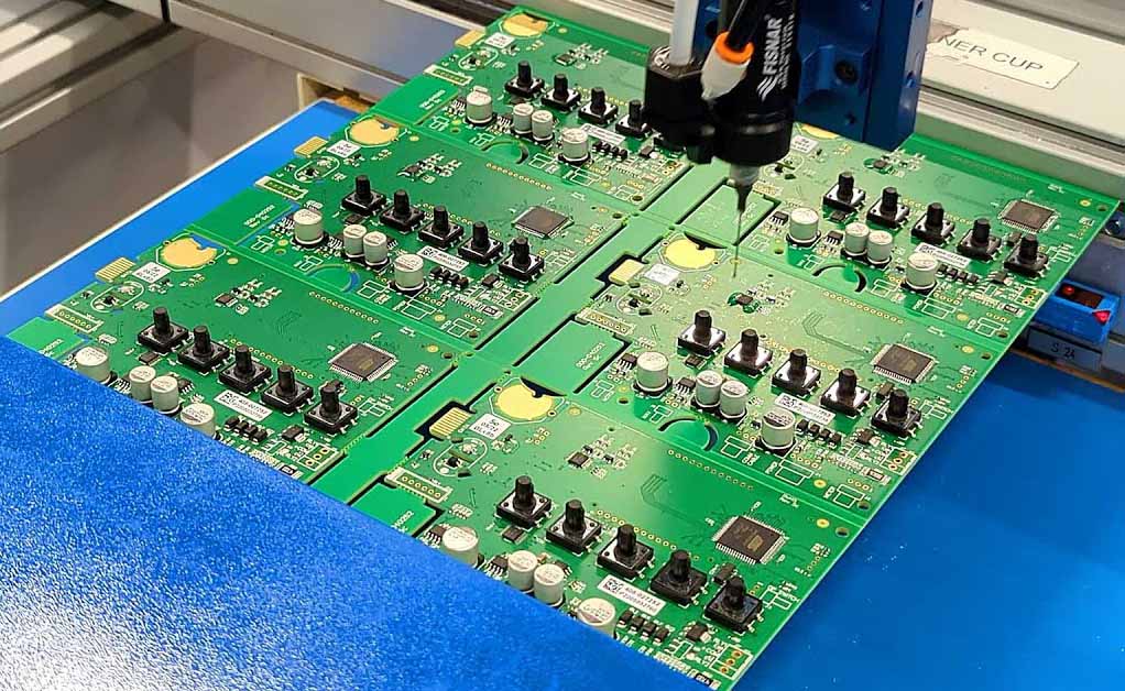
Why is Robotics PCB Assembly Different from Standard PCBA Projects?
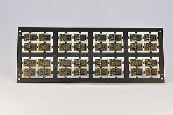
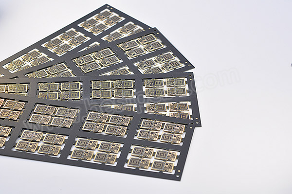
Robotics PCB assemblies combine high-current power stages, fine-tone processors, and often HDI or rigid-flex structures on a single board. The manufacturing tolerance window is narrower than for consumer electronics.
Motor drives generate local heat, while processors require precise flow control. Voids under the thermal pad or uneven solder distribution can compromise performance.
In practice, insufficient stencil optimization leads to poor thermal contact for the MOSFET. Over time, this increases junction temperatures and accelerates failure.
Key assembly control points include:
- Stencil aperture adjustment for electrical devices
- X-ray inspection of BGA and thermal pads
- Controlled reflow profiling
- Selective soldering for through-hole connectors
- AOI calibration for mixed package boards
Nonetheless, AI-enabled robotics introduces greater thermal density and complexity.
When Should You Choose AI Robot PCB Assembly for Advanced Control Systems?
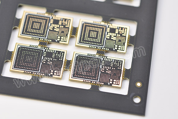
AI robotic PCB assembly is required when edge computing, multi-sensor fusion, and high-speed memory routing demand HDI-level precision.
AI processors require stable, low-noise power rails and controlled impedance routing. Assembly quality directly affects the long-term reliability of the BGA.
In manufacturing, inadequate temperature profiles during the reflow process can create hidden micro-gaps beneath the AI processor. This problem often appears only after a thermal cycle occurs in the field.
Key implementation factors include:
- Verify HDI microvia integrity
- Controlled impedance stack modeling
- Quality control of thermal pad soldering
- Memory routing length matching
- Electrical field segmentation
Therefore, fabrication capabilities must align with the demands of AI-driven systems.
How Does PCB Manufacturing Robot Control Affect System Level Reliability?
Robot control PCB manufacturing determines long-term mechanical durability and electrical stability. Material selection and coating quality influence life cycle performance.
Boards subjected to repeated heating cycles must maintain the integrity and adhesion of the laminate. Materials with low Tg or inadequate copper plating can cause delamination.
In field returns, common failure modes include gap cracking near motor connectors and solder fatigue in high-current zones.
Important manufacturing elements include:
- High Tg laminate options
- Adequate through the thickness of the barrel
- Symmetrical copper distribution
- Final surface consistency
- Controlled board flatness
More importantly, power architecture design plays a decisive role in overall system resilience.
What Power Architecture Considerations Are Most Important in Robot Power PCBs?
Robot power PCB designs must support current surges, battery fluctuations, and regenerative braking without voltage instability.
If the routing power is too small, torque peaks cause a voltage drop and MCU reset. This creates unpredictable system behavior.
During SMT production, thin copper traces and insufficient heat dissipation are often failure points in load testing.
Key points in power design include:
- Selection of copper thickness 2–6 ounces
- Short high current loop
- Optimized MOSFET pad geometry
- Thermal through the array beneath the electrical device
- Powerful decoupling capacitor network
At this stage, high-density routing considerations often arise in advanced robotics systems.
How Will HDI PCB AI Robot Requirements Change Stack-Up and Layout Strategy?
The AI robot’s HDI PCB structure enables compact design and high-speed signal routing but requires precise stacking planning.
Sequential lamination and microvia structures allow dense routing but increase fabrication complexity. Poor stack symmetry causes warping during position changes.
In production lines, improper resin flow control during lamination can reduce microvia reliability, impacting long-term signal integrity.
Design and fabrication factors include:
- Sequential lamination planning
- Controlled impedance modeling
- Laser microvia inspection
- Resin flow management
- Stack symmetry optimization
Ultimately, verification testing validates whether design and manufacturing choices meet field demands.
What Testing Standards Are Required for Robotic PCB Testing in Harsh Environments?
Robotic PCB testing should simulate electrical, thermal, and mechanical stress conditions that reflect actual applications.
Industrial robots encounter vibrations, dust, and temperature variations. Basic ICT alone cannot guarantee its resilience.
In manufacturing practice, burn-in testing and dynamic load simulations reveal marginal boards before shipping.
Key points in the testing protocol include:
- Validation of ICT and FCT
- Thermal cycle testing
- Vibration simulation
- Power load voltage testing
- Extended burning procedure
Overall, measurable production capabilities determine the success of a robotics project.
How to Choose a Robotics PCB Assembly Partner for Scalable Production?
Selecting a robotic PCB assembly partner requires evaluating engineering depth, SMT capabilities, and scalability planning.
A factory experienced in robotics understands mixed signal motor control boards and AI processor integration. Without such experience, yield instability becomes commonplace during scale-up.
In real production transitions, lack of DFM feedback and process control often leads to reduced yields when moving from pilot production to mass production.
The main evaluation criteria include:
- Proven robotics project experience
- HDI and heavy copper fabrication capabilities
- SMT and internal inspection system
- The DFM review process is structured
- Flexible volume scaling capacity
Basically, the success of PCB robotics manufacturing depends on the alignment of techniques from design to production volume.
In short, robotics PCBs are the foundation of movement precision, electrical stability and system reliability in modern automation. Engineering-led design and disciplined manufacturing prevent hidden risks before implementation. Scalable robotics PCB assembly ensures a smooth transition from prototype to production.
For robotics PCB manufacturing and assembly support, feel free to contact us [email protected].
FAQ About PCB Robotics
What is a typical copper thickness for a robotics motor control PCB?
- The motor control zone typically uses 2–4 ounces of copper, depending on peak current demand and thermal design.
Do robotics PCB projects always require HDI technology?
- Not always. Compact, AI-driven systems benefit from HDI, while basic motor controllers may use standard multilayer boards.
How long does robotics PCB assembly take for prototyping?
- Prototype lead times generally range from 7 to 15 days, depending on the number of layers, material availability and testing requirements.
Can robotics PCB production scale from small batches to high volumes?
- Yes, as long as the stacking, sourcing strategy, and SMT process are planned for scalability from the start.
Tags: AI Robot PCB Assembly, Robot Control PCB Manufacturing, Robot Power PCB, Robotics PCB, robotics PCB assembly, Robotics PCB Design
This entry was posted on Monday, March 2, 2026 at 11:48 am and is filed under best PCB, best PCB, HDI PCB. You can follow any responses to this entry via the RSS 2.0 feed. You can skip to the end and leave a response. Ping is currently not allowed.
Berita Terkini
Berita Terbaru
Daftar Terbaru
News
Jasa Impor China
Berita Terbaru
Flash News
RuangJP
Pemilu
Berita Terkini
Prediksi Bola
Technology
Otomotif
Berita Terbaru
Teknologi
Berita terkini
Berita Pemilu
Berita Teknologi
Hiburan
master Slote
Berita Terkini
Pendidikan
Resep
Jasa Backlink
Slot gacor terpercaya
Anime Batch