Why choose PCB polyimide? “This guide detailed the critical nature, thickness, thermal conductivity, pros and cons, manufacturing processes and applications.
Are you still having problems with this problem?
- Complex circuit design leads to low results?
- Traditional materials decline in humid environments?
- Does micro-aperture processing affect the accuracy of the circuit?
The Best Technology ¸¨polyimide PCB Manufacturer in China for 18 years:
- High precision graphic transfer technology: using the direct imaging process of laser (LDI), the width of the line/distance line up to 25îief, the yield increased by 30%.
- Ultra-low water absorption material: 0.2%water absorption formula, isolation resistance retention rate in a humid environment> 95%.
- Processing Micro Hole Precision: CO2 Laser + Laser UV combines drilling, aperture accuracy ± 15îief.
Welcome to contact us if you have a request for PCB Polimida: [email protected].
What is PCB Polimide?
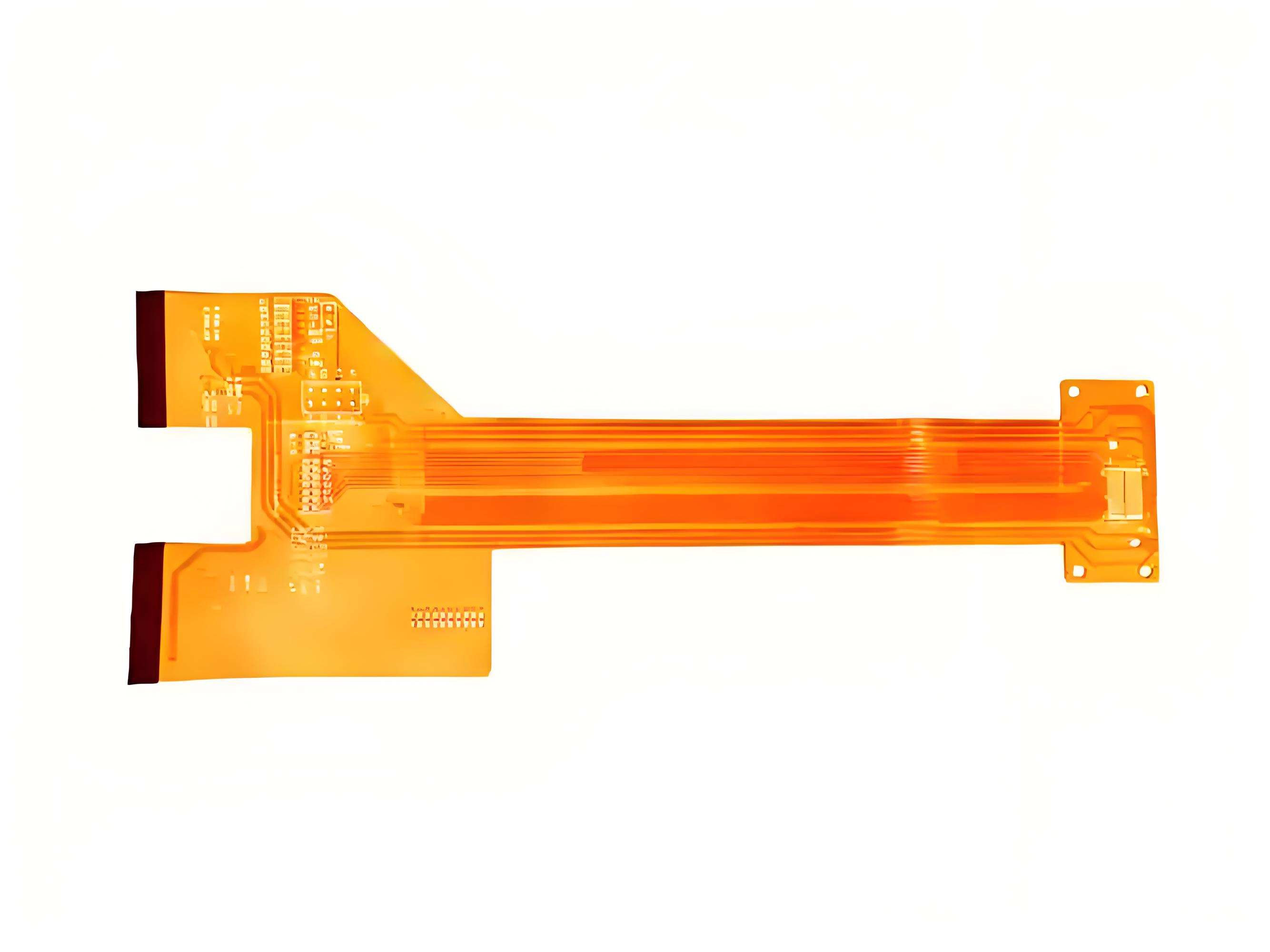
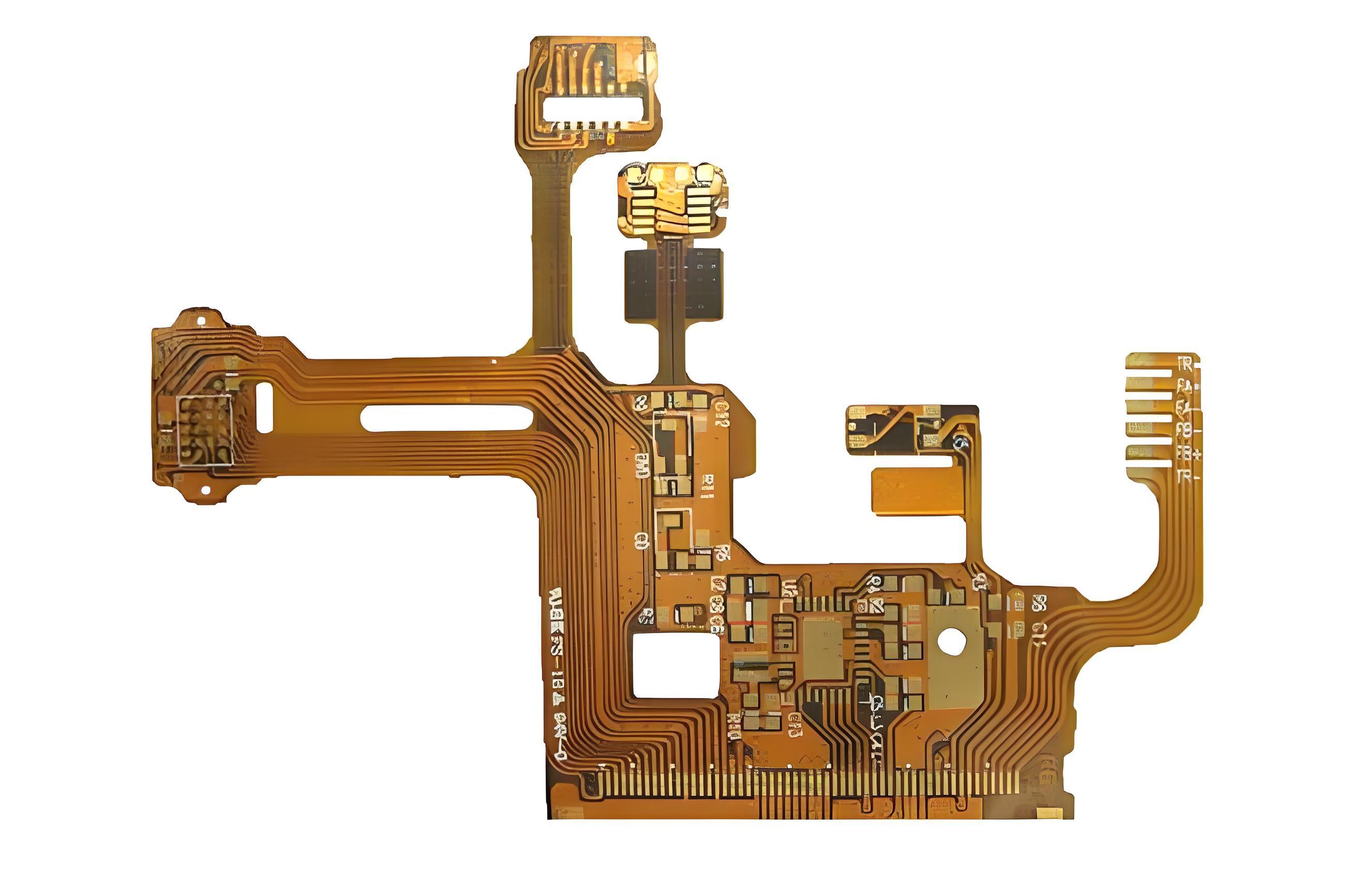
A PCB polyimide Is a flexible print circuit board that uses polyimide as a dielectric substrate, provides extraordinary flexibility for flexible, folding, or turning repeatedly without mechanical damage. This polymer offers extraordinary thermal stability, handling temperatures up to 400 ° C, low dielectric constants near 3.5, and high tensile strength, making it suitable for electronics that require dynamic movements or complicated three -dimensional three -dimensional packaging.
Generally applied in nerve implants and devices that can be used, this PCB allows reliable electricity connections in a limited space while maintaining performance under pressure. Fabrication involves compatible techniques with microelectronics, supporting mass production for high density interconnection in all medical and consumer applications.
How thick is the PCB Polymide?
Core material thickness
- Polyimide base film ‘:: Usually “”12.5 îief to 100 îief (0,0005â € “0.004 inches) â € œwith “25 îief (0.001 inch) “and” 50 îief (0.002 inches) “become industrial standard.
Total Stackup thickness
- Single -layered flexible PCB ‘: “50” 125 “ (0.002 € “0.005 inches)” when combined with copper foil (9 “18”).
- â € œMulti-layer designs’:: The range of â € œup to 0.3 mm (0.012 inches) “for 4” “6 layers Configuration uses adhesive bonds.
Factor affecting
- Copper foilâ € œ:: Ultra-thin “9” 18 îief “The electrodeposition copper reduces large amounts.
- “ Bonding Films adds “10” 25 î¼m ‘per layer; The adhesive lamination reduces the total thickness to “30 îiefm”.
- â € œFuffeners’:: Localized PI or Steel Assistance (“0.1 “0.3 mm”) increase the connector zone.
Sheet & property of polyimide pcb material material
| Property category | Test parameters | Test standard | Value with unit | Characteristics |
| Physical properties | Density | ASTM D792 | 1.43 g/cmâ³ | Light design advantages |
| Water absorption | ASTM D570 | 0.3% | Low humidity absorption for high frequency stability | |
| Flammable ranking | UL94 | Not flammable | Comply with Dirgantara Safety Requirements | |
| Mechanical properties | Tensile strength | ASTM D638 | 90 MPA | 3ã-stronger than the FR-4 substrate |
| Extension at rest | ASTM D638 | 6-8% | High tenacity for dynamic bending applications | |
| Flexible power | ASTM D790 | 98 MPA | Supports the finger design of 5mm bends | |
| Thermal nature | HDT @1.82MPA | ASTM D648 | 360 „ƒ | Hold the solder reflow |
| Sustainable operating temperature. | UL746B | 260 „ƒ | Suitable for automotive electronics | |
| CTE (Z axis) | ASTM D696 | 1-5ã-10 »â µ /â„ ƒ | Matching Copper Foil Expansion (Cu: 17ã – 10⠻ ¶/â„ ƒ) | |
| Electric properties | Dk @1MHz | IEC 60250 | 3.4 | Low signal loss for high frequency transmission |
| Volume resistivity | IEC 60093 | 10¹ · î © Â · CM | 100ã – Isolation is higher than the standard material | |
| Dielectric strength | IEC 60243 | 110-120 kV/mm | Superior high voltage damage resistance | |
| Special performance | Flex Life @5mm radius | IPC-6013D | > 100,000 cycles | Validated in devices that can be worn smart |
| Peel strength (cu foil) | IPC-TM-650 | ‰ ¥ 1.0 N/mm | Ensure the reliability of the flexible circuit | |
| Min. Line width/distance | IPC-2223 | 30/30 îiefm | Ultra-high stomach ability |
What is the thermal conductivity of PCB flexible polymide?
| Type of material | Thermal conductivity | Improvement mechanism |
| Pure Polyimide (PI) | 0.18 W/(mâ · k) | N/A (Basic Material) |
| PI/CNNS Nanocomposite | 2.04 W/(Mâ · K) (+1033%) | CNNS self -orientation in the field |
| Graphene-pi composite | Up to 739.56 W/(mâ · k) | Graphene thermal network layered |
What are the pros and cons of the Polimide circuit board?
Pro (profit) “
- High cable density and miniaturization ‘:: Activate compact design for applications that are limited in space such as mobile devices or items that can be worn.
- Light and thin profileâ € œ:: Reducing the weight and thickness of electronic products as a whole, ideal for portable electronics.
- Very good flexibility and durability. Can withstand millions of dynamic bends without wire damage, supporting complex 3D assembly.
- Flexibility in the spatial layout ‘:: Allows scaling and arbitrary movements in a three-dimensional space for integrated component connections.
- Extensive application “:: Suitable for high fields of reliability such as aerospace, military, and digital cameras because of the strong isolation nature.
Cons (loss) “
- High initial costâ € œ:: The design process, stomach, and photography are expensive due to special manufacturing requirements.
- Limited use for general applications’:: Usually justified only for specific needs, not cost effective for standard PCB.
- Maintenance Challenges’:: Repair and re -work, such as solder, requires trained personnel to avoid damage.
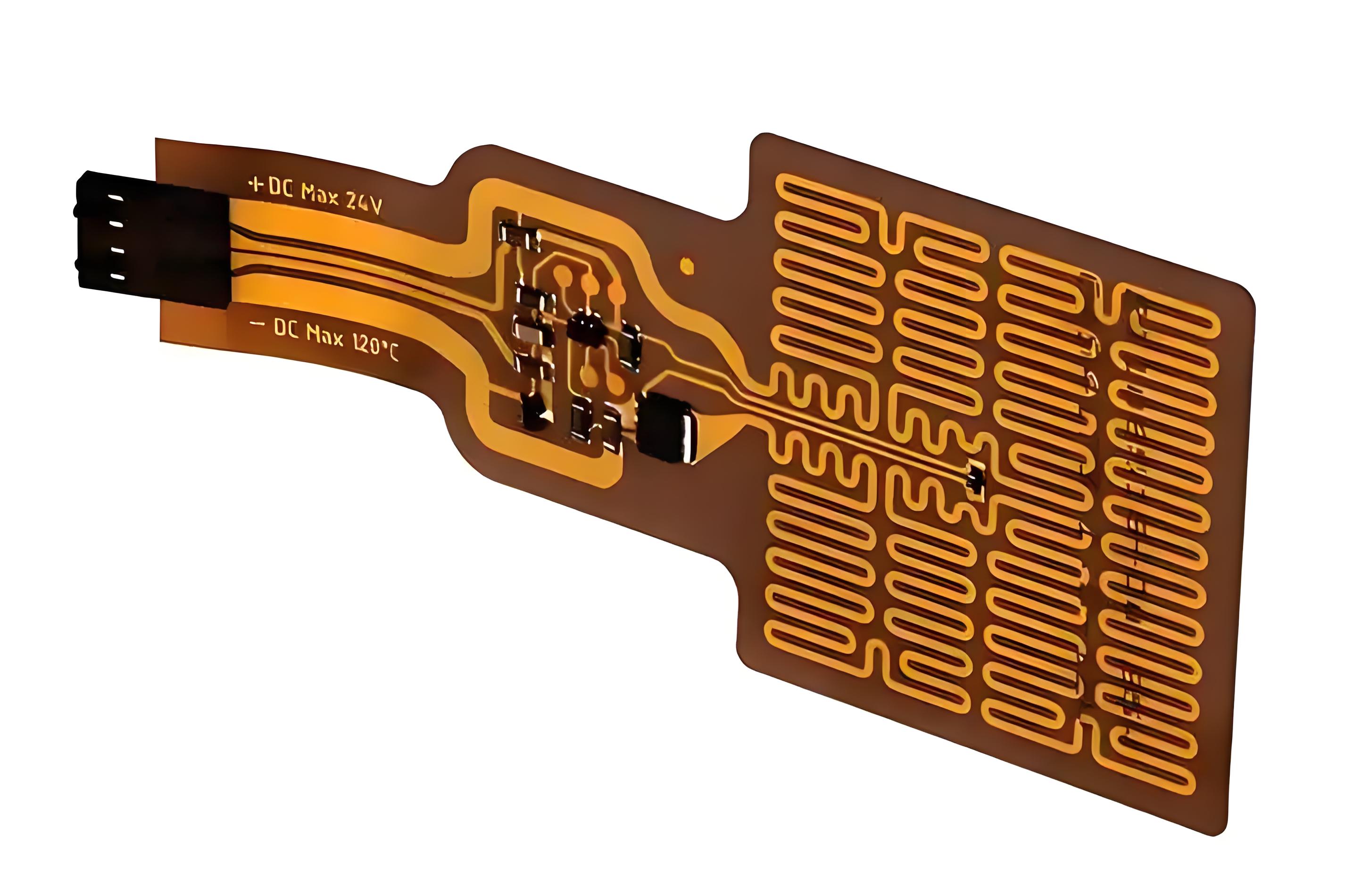
What is the application of PCB Flexible Polymide?
PCB application flexible polymide
- Consumer Electronics – Folding display (smartphone/tablet).
- Aerospace – High temperature wandering on satellites/spacecraft.
- Medical devices – Sensors that can be used (EKG patches/implantable modules).
- Automotive – Battery Management System (EV) & Autonomic Vehicle Sensor.
- Industrial Automation – Flexible joints in the arm control system/robot motion.
- Energy – Solar panel interconnection (flexible photovoltaic module).
- Telecommunications – High frequency signal routing on 5G/mmwave wave devices.
How is PCB polyimide produced?
The process of making a flexible polymide PCB
1. Material preparation
- Basic film: Polyimide (PI) film (12.5â € “50 μm) was chosen for thermal stability (TG> 250 ° C).
- Adhesive layer: Epoxy/acrylic adhesive is applied to the film PI for copper bonds.
2. Cladding copper
- Lamination: The adhesive -plated PI film that is laminated with electrolytic copper foil (1/3â € “2 ounces) in 180 €” 200 ° C.
- Temporary transportation: Aluminum/steel carriers are installed for Ultra-thin FPC to prevent warping.
3. Circuit pattern
- Dry film application: Dry films are laminated photosensitive to copper.
- Exposure & Development: UV lamps explain the circuit pattern; Areas that are not exposed are swept away.
- Etching: Eta ferrik chloride/alkaline removes unprotected copper (width of the line/distance ‰ ¥ 25 µm).
4. Coverlay application
- Pi Covery: The second film with a laminated adhesive on the circuit for protection.
- Laser ablation: Co “laser drill the precision hole (via/pad opening).
5. Coating & Final Surface
- Enig Plating: Nickel gold/electric soaking applied to bearings for solderability.
- Bonding Bonds: The FR4/PI is attached to the connector zone through thermal bonds.
6. Testing & Inspection
- AOI: Automatic optical inspection for defects (open/short circuits).
- Electricity Testing: Flying test/bed nails verify continuity/impedance.
7. Cutting & Formation
- Laser cutting: The formation of precision from the outline of FPC.
- Bending Test: Validation of flexibility (1,000+ bend cycles at 180 °).
8. Final cleaning & drying
- Ultrasonic cleaning: Eliminating residual particles from ETSA/coating.
- Burning: FPC is dried in an 80 “100 ° C oven to eliminate moisture.
9. Packaging
- Anti-static protection: FPC is placed in an anti-static bag with a dryer package.
- Bearing: Foam inserts or trays formed by vacuum used to prevent movement.
- Labeling: Barcode/QR Code Label includes product IDs, batch numbers, and Rohs compliance.
10. Check the final quality
- Visual inspection: Confirm there is no scratches, folds, or contamination.
- Electricity re -testing: Sample testing for critical parameters (for example, impedance).
Polyimide PCB Manufacturer in China – The Best Technology
The reason why choosing us as Polyimide PCB Manufacturer:
- Fast Prototype 24 Hours: Shorten the R&D cycle by 50% and accelerate the launch of the product.
- 1 piece of MOQ: Zero inventory risk, the production cost of trials is reduced by 90%.
- Competitive & transparent prices There is no hidden cost, offering the best value without reducing quality.
- Turnkey Solution â € “Complete PCB Manufacturing Services from Design to Shipping, Speed up the time-to-market of your product.
- ISO 14001/ISO 13485 Certification: Medical/automotive customers are exempt from secondary testing, and compliance costs are reduced by 30%
- Ultra-thin substrate processing 0.075mm: Fold the FPC thickness screen reduced by 40%, and the flexural life reaches 200,000 times.
- Blind mature and buried through technology: Circuit density increases 40%, adapting to the needs of 5G/medical implant modules.
- DFM Analysis (Design for Production) Free: Optimizing the PCB layout to reduce material waste, lower production costs, and avoid the final design revision.
Please contact the best technology if you have questions for PCB polyimide: [email protected]. Look forward to the news from you soon!
Tags: Polyimide Flex PCB, Polyimide PCB
This entry was posted on æÿœœä¸ €, 21 7 æœ Monday, 2025 at 11:37 ¸¸¸Å ˆ and submitted under the best PCB, BestTPCB. You can follow any response to this entry through RSS 2.0 bait. You can leave a response, or trackback from your own site.
Game Center
Game News
Review Film
Berita Olahraga
Lowongan Kerja
Berita Terkini
Berita Terbaru
Berita Teknologi
Seputar Teknologi
Berita Politik
Resep Masakan
Pendidikan
Berita Terkini
Berita Terkini
Berita Terkini
review anime