Print circuit board (PCB) forms the foundation of almost every electronic product today. But how does a design turn into a circuit board that works and works? The answer lies in the detailed PCB fabrication process.
What is PCB fabrication?
The PCB fabrication process refers to the entire series of procedures used to produce naked printed circuit boards from your PCB design files-such as Gerbers, ODB ++, or IPC-2581 format € “into the naked board that is actually ready for assembly. This involves a sequence of strictly controlled steps including the inner layer imaging, etching, lamination, drilling, coating, outer layer image, surface finishing, and final testing.
The fabrication process must be precise and strictly controlled to avoid defects such as misalignment layers, incomplete VIAS, or inconsistent impedance – which can all cause failure.
Step by step the PCB fabrication process
Step 1: Technical Preparation (DFM & Cam)
Before the physical process begins, the fabrication team conducts a design review for manufacturing (DFM). This ensures your file complies with the manufacturer’s capabilities. Then, computer creation software (cam) analyzes and prepares files for production. This step includes:
- Stackup layer analysis
- Optimization of drill files
- Netlist extraction
- Validation of Gerber
Step 2: Internal layer imaging
Each inner copper layer is made of copper wrapped lamination coated with photoresis that is sensitive to light. Laser Direct Imaging (LDI) is used to expose the desired circuit pattern to the photoresist. After UV exposure, the area that was not exposed was swept away during the developing stage, revealing the pattern of the copper footprint underneath.
Step 3: ETSA and Strong Strong
Copper that is chemically exposed is eliminated using ETSA solution, such as ammonium persulfate. Hard photoresis protects the copper that must remain. After the ETSA is finished, the photoresist is stripped, leaving the layout of the final copper trail on the inner layer.
Step 4: Inspection and punching the inner layer
Automatic optical inspection (AOI) is carried out on each inner layer to detect shorts, open, or wide variations. After being approved, the layer is beaten optically with the right target to ensure the registration of perfect layers during lamination.
Step 5: The oxide layer for bonds
Before laminate, oxide treatment (or alternative bond methods such as black oxide or alternative oxide) are applied to increase the roughness of copper surfaces. This increases resin adhesion and mechanical strength between layers.
Step 6: Lamination
The core layer and prepreg of copper patterned are stacked sequentially based on the final stack-up design. Using a laminated press, heat bound and the pressure of these materials becomes a multilayer PCB. The shift in any layer during this step can cause disaster disappointment, so that the right registration is very important.
Step 7: drilling
Drilling creates interconnection between layers, including holes and VIAS. High -speed CNC drilling machines are used for standard holes, while laser drilling is used for microvias on PCB HDI. After drilling, the panel experiences deburring and desmearing to clean the hole wall.
Step 8: Electric copper coating
The holes that are drilled are non-conductive at first, so that the thin layer (~ 1 μm) copper is chemically deposited by the surface of the panel and hole walls. This electric copper coating is very important to enable conductivity in all layers of the board.
Step 9: Outer and Electroplating Layer Imaging
The outer layer is also coated with phoresist and exposed through LDI, defining where copper must remain. After exposure and development, the board is replaced with copper to build an outside trace and fill through the hole. The tin coating was then applied as a temporary ETSA detention.
Step 10: The outer layer of ETSA and tin stripping
Open areas (not protected by tin) are carved to eliminate excess copper. After the ETSA is finished, tin is chemically stripped, leaving the right copper pattern for the outer layer.
Step 11: Solder Mask, Silkscreen, and Final Surface
The board is coated with a solder mask to isolate and protect copper traces while preventing the soldering bridge during assembly. Then, silkscreen (legend) is printed to mark component reference designers. Finally, the surface layer is applied to all bearings that are open to improve the ability of solder and protect against oxidation. The typical final results include:
- Enig (Electric Nickel Soaking Gold)
- HASL (Hot Air Soldering Leveling)
- Silver immersion
- Hard gold coating
- Soft gold coating
- OSP (Organic Solder Preservative)
Step 12: Electricity Testing
All artificial boards undergo electricity testing to validate continuity and isolation of the circuit. These include:
- Open/short detection
- Impedance testing (for high -speed circuits)
Testing methods such as flying probes or beds based on volume and complexity
This test confirmed that the final PCB function was exactly as designed.
Step 13: Profiling, Stomach, and Score V
The final step in the PCB fabrication process is a mechanical profile. The board is separated from the panel using a CNC routing, V, or punching, depending on the panelization method. This step defines the exact outer dimensions of each PCB, matching the mechanical image of the customer.
Quality control in the PCB fabrication process
Quality control (QC) is an important part of the PCB fabrication process, ensuring that each board meets design specifications and performance standards. At each stage of production, strict testing and inspection is carried out to prevent defects and maintain reliability.
Main quality control practices include:
- Design Rule Checks (DRC): Done during the cam to validate the width of the trail, distance, hole size, and consistency of the pile before fabrication begins.
- Automatic Optical Inspection (AOI): Used after the inner and ETSA imagery to catch shorts, open, and track problems.
- X-ray inspection: Applied to the multilayer board and HDI to verify the registration of layers and detect internal problems or coating.
- Solder Mask Registration Check: Make sure the solder mask is in harmony with copper pads to avoid bridging.
- Final Surface Evaluation: Verifying the integrity and final thickness of Enig, Hasl, or OSP.
- Electricity testing (e-test): Confirm electricity connectivity from all nets and the absence of shorts through flying probes or bed testing.
- Last Visual Inspection: Technicians visually check boards for cosmetic defects such as soldering masks, blurred silkscreen, or mechanical damage.
In the best technology, we apply 100% inspection rates before shipping, including impedance and verification controls, supported by ISO9001, ISO13485, IATF16949, and AS9100D certification.
General challenges and how to avoid it in PCB fabrication
The PCB fabrication process involves more than a dozen steps that are closely coordinated, and even small deviations can cause functional failure or loss of yield. Understand the most common challenges – and how to prevent it – very important for design engineers and buyers.
1. Misalignment layer
During lamination, even a few registration errors between the inner layer can cause through escape or impedance. This is often due to bad tools, inaccurate punching, or thermal distortion. To avoid this, the manufacturer must use an optical boxing system and control the temperature profile tightly during lamination.
2. inconsistent coating in the holes
Uneven thickness thickness can cause poor conductivity or crack under thermal pressure. This usually comes from the chemistry of the wrong bath or preparation of a bad hole. Electric copper coating, followed by a well -regulated electrolytic coating, is very important to make reliable interconnection.
3. Solder Mask Misalignment
If the solder mask is not accurately registered, he can expose a trail or cover bearing, which leads to a bridging solder. Using laser direct imaging (LDI) for mask solder increases accuracy significantly.
4. ETSA defects
Excessive Rarrows traces; Leaves under etching shorts between conductors. These problems often arise from old chemistry or poor agitation. Producers must maintain strict control over ETSA parameters and regularly calibrate their lines.
5. Warpage on the multilayer board
PCB Calculation of high layers or boards with uneven copper distribution can be curved during lamination or reflow. This is reduced by a symmetrical pile design and consistent copper balance.
The best way to avoid this problem is to partner with producers who offer an initial technical review, monitoring of real-time processes, and full transparency during production.
How do I choose a reliable PCB fabrication partner?
1. Your manufacturer must be able to support the complexity of your design-is it HDI, controlled impedance, via-in-PAD, or metal-pcb. Check the minimum trail/space, number of layers, and material compatibility before continuing.
2. Experienced fabrication partners not only produce what you send. They must actively review your design, EQ feedback files (engineer questions), flag production problems, and suggest an increase in layout. Free DFM reviews, pile optimization, and impedance modeling are the main indicators of capable suppliers.
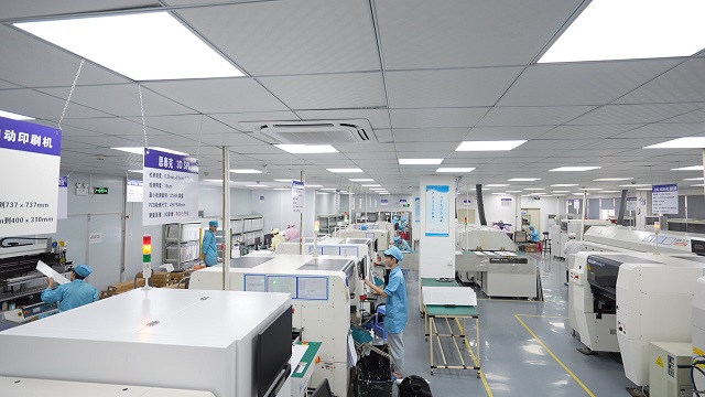
3. Leading manufacturers use the MES system to track each step of your order – from raw materials to final inspection.
4. Ask Your PCB Manufacturer: Can you reach engineers when problems arise? Do you get weekly updates or have to follow up several times? Strong partners maintain open and proactive communication, especially for urgent or high reliability projects.
5. Choose PCB fabrication partners that can handle fast prototypes and volume production.
The best technology is the leading PCB manufacturer in China, we help customers from prototypes to mass production by:
✅ Fast turn 24 hours
✅ Competitive price
✅ Full traceful using the mes system
✅ Technical support for stack-up, impedance, and dfm
Whether you design a six -layer communication board or one -layer aluminum LED module, we can support each stage of your PCB fabrication process.
Frequently asked questions (FAQ)
1. What is the difference between PCB fabrication and PCB assembly?
Fabrication creates a naked board; The Assembly installs components upwards.
2. How long is the PCB fabrication process?
The standard waiting time is 5â € “7 days, but the fast rotation option (24-48 hours) is available.
3. Which surface finish should I choose for my PCB?
Enig is preferred for SMT and Fine-Pitch components; Hasl works well for a hole.
4. Can I ask for a special pile for impedance control?
Yes, the best technology supports a special pile for RF boards, high -speed, and HDI.
5. How much does the PCB fabrication process cost?
Costs depend on the number of layers, board size, material, final layer, and waiting time.
Tag: PCB fabrication process
This entry was posted on Wednesday, June 11, 2025 at 18:03 and submitted under the best PCB, BestTPCB, FAQ, FR4 PCB, PCB News, PCB Technology. You can follow any response to this entry through RSS 2.0 bait. You can leave a response, or trackback from your own site.
Game Center
Game News
Review Film
Berita Olahraga
Lowongan Kerja
Berita Terkini
Berita Terbaru
Berita Teknologi
Seputar Teknologi
Berita Politik
Resep Masakan
Pendidikan
Berita Terkini
Berita Terkini
Berita Terkini
review anime
Gaming Center
Originally posted 2025-06-11 21:53:08.