Etsa is one of the most important steps in making a printed circuit board (PCB). This is a process that removes unwanted copper, leaving a clean circuit trail. Whether you build a PCB for new projects or manufacturing on a scale, understanding the workings of the PCB ETSA helps you get better quality and less production problems.
In the best technology, we are specializing in high precision PCB fabrication. From prototype to volume production, our team follows strict quality standards to ensure high -quality PCB. Now let’s look closer to the PCB ETSA process.
What is ETSA PCB?
ETSA PCB is the process of eliminating the excess copper from a copper wrapped board to form the desired circuit pattern. This is usually done after the copper layer is covered with Etch resistant masks, which protect certain areas during ETSA. Only unprotected copper dissolved by Etchant solution.
ETSA created a trace of the circuit that connects electronic components. If done incorrectly, you can end in a broken trail, short circuit, or an unreliable connection. That is why it is important to understand the whole process before starting.
What liquid is used for PCB ETSA?
Some chemical solutions are generally used for PCB ETSA, depending on the scale of production and thickness of copper. The most commonly used liquid includes:
- Ferric Chloride (Fecl₃): Traditional etchant used for simple PCBs or hobbies. This is affordable but stains and difficult to throw.
- Ammonium persulfate (nhâ “”) “” “o”: produces cleaner results with fewer chaos. Suitable for small -scale production.
- Cupric chloride (Cuclâ ‚): common in the industrial PCB ETSA line. It offers consistent results and can be regenerated for reuse.
- Etchant Alkali: This is used in professional PCB stores. They give high -speed etching and better line resolution.
Each etchant has different properties, such as the rate of ETSA, temperature sensitivity, and compatibility with detention. Industrial PCB manufacturers often choose the most suitable with the width of the line, the thickness of copper, and the standard of environmental compliance.
What materials are needed for PCB ETSA?
Before starting the ETSA process, you will need the following material:
- Copper rated laminate: This is a raw board, coated with a thin layer of copper.
- ETSA Solution: Ferric Chloride, Cupric Chloride, or other chemical agents.
- A resistant layer to ETSA: usually photoresis or screen printing printed to cover the pattern.
- Developer Solutions (if using Photoresist): Helps reveal the resistant pattern before ETSA.
- Protective equipment: gloves, glasses, and smoke protection to deal with chemicals safely.
- Etsa tank or tray: to soak and process board evenly.
- Agitation System: Helps increase the speed and consistency of ETSA (manual or automatic).
- Rinse Station: To stop chemical reactions after ETSA and remove residues.
These ingredients work together to protect circuit patterns and eliminate unwanted copper with high precision.
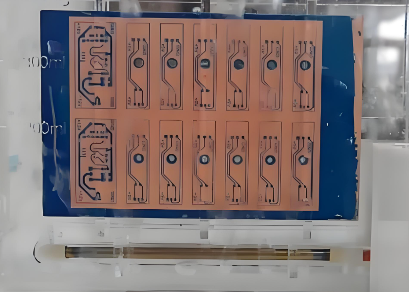
PCB ETSA Process
The PCB ETSA process is one of the core steps that converts the laminate that is dressed in copper into a functional print circuit board. This defines a copper trail that carries electrical signals between components. The purpose of ETSA is to remove all unwanted copper from the board, leaving only copper paths protected by the resistant layer.
1. Surface preparation
Before the ETSA begins, the copper surface must be fully clean and free of oxidation or oil. Any contamination can prevent rejection from sticking properly. Most producers use mechanical rubbing or chemical cleansing (such as acid dyeing) to ensure a uniform surface.
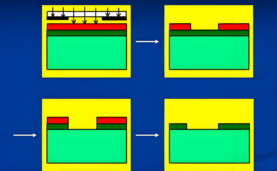
2. Apply the resistant layer
After the board is clean, the protective layer called the resist is applied to cover areas that should not be carved. There are several ways to apply resistant:
- Dry Film Photoresist (DFR): laminated using heat and pressure.
- Liquid Photoresist: sprayed on the board.
- Screen printing: used in simple PCB or low resolution.
For most precision PCBs, photoresists are preferred. This allows for fine and compatible line resolution with automatic processing.
3. Exposure and development
After the resist application, the board is harmonized with phototool or artwork ”a transparent film with the desired circuit pattern. The board is then exposed to UV rays, which hardened detention in the area exposed to light. The rest remains soft.
The board is then placed in a developer solution, which eliminates uncovered rejection (not exposed). This reveals the copper that will be engraved, while protecting the traces and pads under the hardened resistan.
4. ETSA
The board enters the ETSA room, which is sprayed or soaked with a chemical solution designed to dissolve open copper.
Depending on the production scale and type of PCB, different etching systems are used:
- Soaking etching: The board is dipped in the etchant tub. Simple but slower.
- ETSA spray: High pressure nozzles Etchant spray uniformly throughout the board, giving faster and more controlled etc.
- ETSA Machines are converted: used in mass production, offering precision and speed.
The most common etah chemicals at this stage include:
- Alkali cupric chloride (cuclâ, “): efficient and widely used in high -speed lines.
- Ammoniacal etchant: offers faster etching, especially suitable for fine line PCBs.
Etsa is a process that is sensitive to time. Too short, and some of the remaining copper. Too long, and the resist can lift, which leads to undercutting or tracking erosion.
5. Etch quality control
Quality examination is very important after ETSA:
- The width of the line and the distance inspection ensures the trail matches the design in question.
- The cross section test confirmed the thickness of copper in tolerance.
- Undeletch detection helps avoid electric shorts and performance problems.
Upper -class manufacturers such as the best machine use an AOI engine (automatic optical inspection) to check each board for ETSA defects at this time.
6. Larched the resist
After the ETSA is finished, the remaining photoresis is no longer needed. Deleted using a chemical resist stripper, expressing a clean and shiny copper trail.
This step is preparing a board for further processing such as mask solder applications, drilling, or final layer of surface (such as Enig or Hasl).
7. Rinse and neutralize
After stripping, the board undergoes a comprehensive rinsing process using water deionization to eliminate any chemical residue. Neutralizing agents can also be applied to balance the pH level and prevent corrosion.
How long does it take to carve a PCB?
ETSA time depends on several factors, such as:
- Copper thickness: a thicker copper layer takes longer for ETSA.
- Etchant Concentration: A higher concentration speeds up the process.
- Temperature: a warmer solution increases the rate of ETSA.
- Agitation: Moving solutions or boards increases uniformity and speed.
Usually, Etsa hobby using Ferric Chloride can take 10â € “30 minutes, while the alkaline industry etching can be completed in 1â €” 3 minutes with consistent results. Time control is very importantâ € “over-etching can cause side and weak traces.
Calculation method for PCB etc.
Professional PCB manufacturers use formulas to calculate etching factors, which help balance speed and precision. Etch (EF) factors are:
EF = ETCH depth / Undercut distance
High ETSA Factors means more vertical etching (cleaner side walls), while low etching factors indicate more lateral etching (side erosion). This factor helps adjust etchant chemistry and exposure arrangements.
Key parameters include:
- Ethant Type and Strength
- Temperature control
- Agitation method
- Line width and distance
- Copper thickness
By adjusting this parameter, producers can maintain strict tolerance and maintain traces of loyalty even on high density PCBs such as HDI boards.
What should I do if the PCB side etching occurs?
Etsa Side occurs when Etchant cuts under the resist, reducing the width of the trace and weakening the circuit. This is a common problem with a long etching time or the wrong resistal application.
To reduce or eliminate side etching:
1. Use the right Photoresist application: Make sure full coverage and adhesion to copper.
2. Optimizing exposure and development time: backward or excessive resistant can be removed during ETSA.
3. Shorten the duration of ETSA: Use stronger etching or increase agitation to reduce the total time of ETSA.
4. Increase the direction of ETSA: ETSA spray is better than soaking for fine features.
5. Apply protective overcoats: for high precision PCB, hard resistant layers or dry films help.
In production, engineers often run test coupons with real boards to monitor the quality of ETSA in real time.
Choose the Best Technology Professional PCB Partners
In the best technology, we handle complex PCB ETSA challenges with sophisticated production pathways and strict quality control. We support everything, ranging from a simple single -coated PCB to Multilayer HDI PCB, flexible circuit, and even ceramic -based PCB. Our MES system tracks the ETSA process of each board for full tracking.
Do you need prototype fabrication or mass production, we guarantee:
- High ETSA precision
- Clean edge definition
- Minimal side etc.
- Consistent quality for fine-pitch circuits
Looking for a reliable PCB ETSA service? Contact the best technology today and start your project with confidence.
FAQ
1. What is the safest etchant for use at home?
Ammonium persulfate is cleaner and less messy than iron chloride, although both require safety prevention measures.
2. Can I reuse the PCB ETSA solution?
Yes, some etching such as cupric chloride can be regenerated, but they need careful chemical control.
3. What causes uneven etching?
Poor resisting applications, inconsistent agitation, or expired chemicals can cause patchwork ethics.
4. How to clean the PCB after ETSA?
Rinse with water, then clean it with isopropyl alcohol to remove the remaining residues before applying a soldering mask.
5. Is photoresis better than screen printing for masking?
Phoresists offer a higher resolution and are preferred for PCB Pitch or Multilayer designs.
Tag: ETSA PCB, ETSA PCB Process
This entry was posted on Friday, June 20, 2025 at 18:31 and submitted under the best PCB, BestTPCB, FAQ, FR4 PCB, PCB Technology. You can follow any response to this entry through RSS 2.0 bait. You can leave a response, or trackback from your own site.
Game Center
Game News
Review Film
Berita Olahraga
Lowongan Kerja
Berita Terkini
Berita Terbaru
Berita Teknologi
Seputar Teknologi
Berita Politik
Resep Masakan
Pendidikan
Berita Terkini
Berita Terkini
Berita Terkini
review anime
Gaming Center
Originally posted 2025-06-20 22:55:45.