If you have ever held a green circuit board, you might see a PCB FR4. This is one of the most common ingredients used in the production of the current printed circuit board. But what makes FR4 so popular? And how exactly the process of making PCB FR4 works from beginning to end?
In this guide, we will guide you through everything from the basics of FR4 material to the full production process, the design of the PCB FR4 stack-up, the material nature, and the main manufacturing considerations. Whether you are a designer, engineer, or purchase specialist, this is your reference to work with PCB FR4.
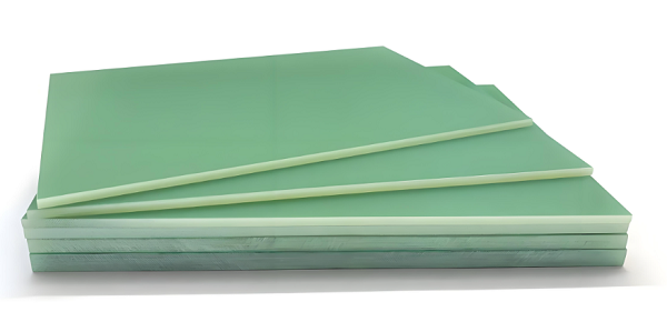
What is FR4 material?
FR4 is an abbreviation of “Flame Retardant 4. € This is a type of epoxy laminate that is strengthened by fiberglass that meets certain fire resistance standards. The core of this material is made of woven fiberglass fabric soaked in epoxy resin. This combination provides excellent strength and mechanical insulation.
It offers great mechanical strength and excellent isolation, even at high temperatures. Because of these quality, FR4 PCB materials are widely used in everything ranging from cellphones and automotive systems to medical devices and industrial control.
FR4 PCB Material Property
Any PCB performance starts with the basic ingredients. This is what makes the nature of the PCB FR4 material suitable for various electronics:
- Electric insulation: FR4 is an excellent electrical insulator, which protects your circuit.
- Heat Resistance: This can hold solder and other high temperature processes.
- Mechanical strength: The fiberglass base provides structural durability.
- Moisture resistance: FR4 does not absorb a lot of water, so it remains stable in humid conditions.
- Thermal stability: Most of the FR4 material can handle temperatures up to 130 ‘”140 ° C. Some versions of TG are higher higher.
FR4 PCB Stack-Up
Stack-up refers to how the layer of copper and insulation is regulated in a PCB. In PCB FR4, the pile directly affects the performance of signals, EMI control, and even thermal management. The typical FR4 PCB pile can have one, two, or several copper layers separated by the dielectric layer FR4.
The basic PCB FR4 pile may include:
- Top copper layer (signal)
- Prepreg layer (dielectric made of FR4)
- Deep copper layer (for power routing or signal)
- Core (FR4 material with copper on both sides)
- Lower copper layer
For multilayer boards, additional layers are added between the upper and lower layers using a back and forth of copper and Dielectric-based FR4.
Engineers design piles based on signal integrity, board thickness, and power distribution requirements. Choosing the right settings increases reliability and helps prevent signal disorders.
FR4 PCB thickness
One important design decision is to choose the right thickness of the FR4 PCB. Standard boards are often 1.6 mm thick, but other options are available, ranging from 0.2 mm to more than 3.2 mm.
FR4 boards usually come in standard thickness such as:
- 0.4 mm
- 0.8 mm
- 1.0 mm
- 1.2 mm
- 1.6 mm (most common)
- 2.0 mm
Special thickness is also available depending on the application. Thicker boards are ideal for mechanical strength and high -current application, while thinner boards are used in compact devices such as smartphones.
When choosing the thickness of the PCB FR4, consider the following:
- Mechanical strength: thicker boards provide more durability.
- Flexibility: thinner boards can reduce weight and size.
- Thermal load: more copper and greater thickness helps eliminate heat.
- Signal integrity: The distance between the signal layer is important in high -speed design.
Appropriate thickness planning improves performance and reduces warping during reflow or wave solder.
What is the difference between FR4 and FR5 PCB?
At first glance, the materials of FR4 and FR5 may look very similar to their two fiberglass -based substrates. However, the main difference lies in their thermal performance.
| Owned by | FR4 | FR5 |
| Max Temp. Resistance | ~ 130â € “140 ° C. | ~ 170â € “180 ° C. |
| Cost | Lower | Higher |
| Application | General Electronics | High temperature environment |
| Dielectric strength | Tall | Comparable to FR4 |
FR5 is a FR4 version that is more tolerant of heat but is also more expensive. Unless your project involves high temperatures, FR4 will usually be a better choice. Most consumer and industrial electronics use FR4 unless extreme thermal demand requires an increase to FR5.
FR4 PCB Manufacturing Process – step by step
Now we have discussed material considerations, buildup, and design, let’s explain the entire process of making PCB FR4.
1. Material preparation
Manufacturing begins with choosing the right FR4 board based on the desired thickness and copper weight. The sheet is cut into panels and cleaned to be processed.
2. Internal layer imaging
For Multilayer PCBs, the copper layer is carved first. Fotoresis is applied, and the circuit pattern is transferred using UV lamps. Unwanted copper is engraved using a chemical solution.
3. Layer of alignment & lamination
After the inner layer is engraved, the layer is stacked with prepreg (uncurable FR4 resin sheets) between them. This stack is laminated under the heat and pressure to bind all layers together.
4. Drilling
Next, the hole is drilled for VIAS and components through the hole. High -speed CNC machine or laser drill is used depending on the design.
5. Plating
The holes that are drilled are chemically treated and then coated with copper. This forms a conductive path between layers.
6. Imaging & ETSA Outer Layer
The outer copper layer through the equivalent process and the same ETSA as the inner layer. The circuit pattern is made using photoresis and chemical etc.
7. Solder Mask Application
The protective solder mask is applied to isolate copper traces and prevent the soldering bridge. This step also gives a green board (or sometimes blue, red, or black).
8. printing silkscreen
Labels and identification of components printed on the board using white epoxy ink.
9. Surface is complete
The end of the surface such as Hasl, Enig, or OSP is added to open copper pads. This step increases the ability of solder and protects copper.
10. Routing and V-Cutting
The board is cut into the final shape using a router or V-Cut engine.
11. Electric testing
Each board is tested for shorts, opens, and other errors using a flying probe or equipment -based examiner.
12. Final Inspection and Packing
The board is visually checked and packaged in anti-static materials for shipping.
Consideration during making PCB FR4
There are several factors to remember when producing with FR4:
- Thermal Expansion: Consider the coefficient of thermal expansion, especially for multilayer or BGA design.
- Glass Transition Temperature (TG): TG FR4 which is higher is better for soldering applications and lead -free automotive.
- Thickness control: Even small deviations in the thickness of PCB FR4 can affect impedance and performance.
- Copper weight: heavier copper requires more precise etc. and laminated processes.
- Moisture content: Pre-making FR4 panels eliminate trapped moisture that may affect the soldering.
If you work with a reliable FR4 PCB manufacturer, this detail is usually handled with tight quality control.
Why choose the best technology for your FR4 PCB manufacturing?
In the best technology, we specialize in high quality PCB manufacturing using FR4 material. Whether you need a simple prototype or a complex multilayer design, our team provides quality that is consistent with fast turnover. We use an advanced mes system to track your PCB through every production step, ensuring lacking and precision.
We offer:
- Special PCB thickness option FR4
- Expert FR4 Stack-Up Engineering
- Tackling mes in all stages of production
- Fast turnover and competitive prices
- IPC Class 2 and Class 3 Builds Available
If you are looking for a trusted partner for your FR4 PCB needs, our technical team is here to help you from prototype to mass production.
FAQ
1. What is the thickness of the standard FR4 PCB?
The most common thickness is 1.6 mm, but can range from 0.2 mm to more than 3.2 mm depending on the application.
2. Can FR4 be used in high temperature applications?
The standard FR4 supports temperatures up to 140 ° C. For higher temperatures, FR4 or FR5 is recommended.
3. How many layers can PCB FR4 have?
PCB FR4 can have 1 to more than 20 layers depending on the design needs and manufacturing capabilities.
4. What is the difference between FR4 and Cem-1?
CEM-1 is a lower-cost alternative with fewer mechanical strength and limited to a single layer design, unlike FR4 that supports multilayer boards.
5. How long is the process of making PCB FR4?
The waiting time varies from 2 to 10 working days based on the complexity, quantity, and requirements are complete.
Tag: PCB FR4 Making Process
This entry was posted on Friday, May 30, 2025 at 17:39 and submitted under the best PCB, BestTPCB, FAQ, FR4 PCB, PCB News. You can follow any response to this entry through RSS 2.0 bait. You can leave a response, or trackback from your own site.
Game Center
Game News
Review Film
Berita Olahraga
Lowongan Kerja
Berita Terkini
Berita Terbaru
Berita Teknologi
Seputar Teknologi
Berita Politik
Resep Masakan
Pendidikan
Berita Terkini
Berita Terkini
Berita Terkini
review anime
Gaming Center
Originally posted 2025-05-31 20:18:32.