What 3 OZ Copper PCB? Let’s explore the thickness, current capabilities, advantages, applications, design guides, and how to get offers for 3 OZ copper PCB.
Are you having a problem with this problem?
- PCB temperature rises uncontrollably in current conditions. How can I overcome the hot dissipation bottleneck?
- What should I do if impedance fluctuations increase the level of beet errors during high frequency signal transmission?
- The level of compliance with copper thickness for multilayer boards is low after lamination. How can I ensure a consistent quality?
The best technology can provide solutions:
- The process of filling micro-etsa + electroplating: using a surface treatment technology that is owned, we reach the tolerance of 3oz copper thickness â ± 8îiefm, increasing the efficiency of heat dissipation by 40%.
- Simulation of impedance and compensation design: Providing pre-DFM analysis services to proactively compensate for the impact of copper thickness on impedance, ensuring signal loss <3DB
- Vacuum laminate Smart Temperature Control System: Using a segmented pressure process to eliminate the problem of delamination in heavy copper wrapped plates, maintaining a stable yield rate above 98.5%.
Welcome to contact us if you have a request for 3 OZ copper pcb: [email protected].
Is that 3 OZ Copper PCB?
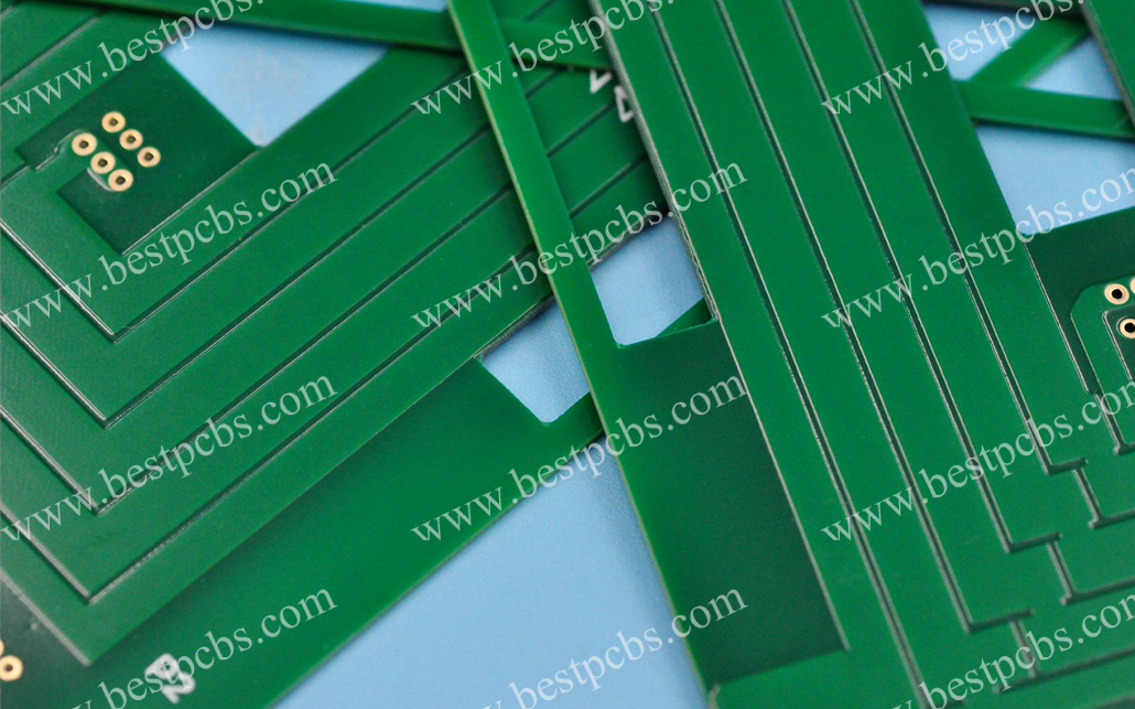
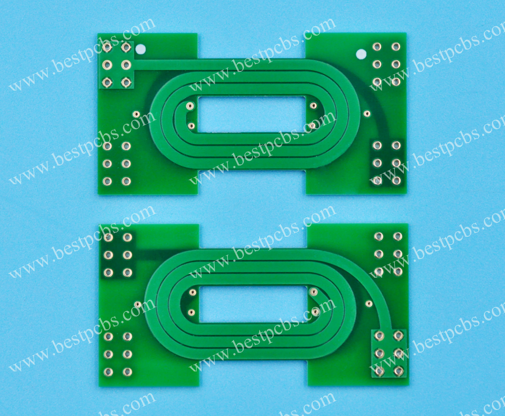
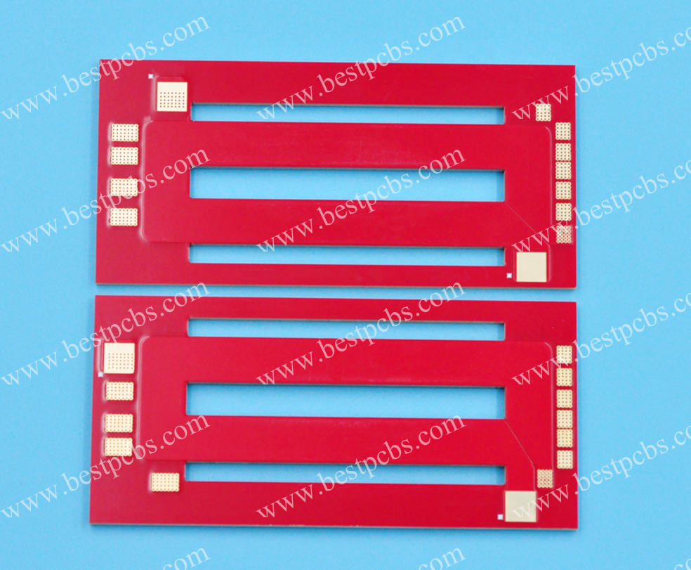
A 3 OZ Copper PCB is a type of “”Heavy copper pcb ‘ Which has a thickness of 3 ounces of copper per square foot, significantly thicker than PCB 1 ounce (35 μm) standard. This design is ideal for high power applications, such as power supplies, automotive electronics, and industrial equipment, where it can handle higher current loads, eliminate more effective heat, and increase mechanical resistance. Increasing the thickness of copper also reduces resistance and improves thermal management, making it a reliable choice for demanding the environment.
How thick 3 ounces of copper on the PCB?
3 ounces of copper on the PCB measuring Kira -Kira 105 micrometers (Μm) Thickness, equivalent to 4.13 miles, which is three times thicker than the standard 1 oz (35 μm) copper foil. This thickness is calculated based on copper weight per square foot, where 1 ounce is equal to 28.35 grams spread more than 1 square foot (0.0929 m²), with 3 ounces representing three times the density of mass.
What is the 3 oz copper PCB current?
3 ounces of copper PCB (105 μm) can usually handle 22â € “30A per 1mm width at an increase in temperature of 20 ° C, depending on whether the trail is in the inner or outer layer (inner layer: ~ 22a/mm; outer layer: ~ 30a/mm). This capacity comes from the standard IPC-2221, which considers the thickness of copper, traces, and an permitted temperature rise. For example, a 10mm width trail on the outer layer theoretically can carry 300A with the right thermal management.
Why Choose 3 OZ Copper PCB?
- Current capacity is higher “Supports up to 30A/mm in the outer layer, allows stable operations for high power applications without excessive heating.
- IMPROVING THEMAL MANAGEMENT “Thicker copper eliminates heat more efficiently, reduces thermal voltage and extending the life of the component.
- Increased endurance “Rejecting mechanical stress and thermal cycles better than thinner copper, ideal for demanding the environment.
- Space efficiency â € “allows a wider or fewer layer of traces in high -current design, simplifying the PCB layout and reducing costs.
- Reliable performance “Minimizing the decrease in voltage and signal loss, ensuring consistent power delivery in industrial and automotive applications.
When to use 3oz copper PCB?
- High current application: Power supply, motor controller, battery management system (BMS), and solar inverter requires thick copper (3oz) to minimize resistive losses and manufacturing heat under heavy loads.
- Critical System of Thermal Management: The automotive engine control unit (ECU), industrial power converter, and LED drivers use 3oz copper to increase heat dissipation, reduce dependence on external heatsinks.
- RF/Microwave power amplifier: A thick copper layer increases the current treatment in a high frequency power circuit, minimizing the loss of signals and thermal voltage in the communication system/wireless radar.
- Mechanical environment: Aerospace PCB, military, and automotive are subject to vibrations, shocks, or thermal cycles using 3oz copper for structural durability and reduced risks of trace fatigue.
- Corrosion resistant electronics: Marine, industrial, and outdoor devices benefit from thicker copper resistance to moisture, salt, and chemical exposure, ensuring long -term reliability.
3 oz copper pcb design guide
Below this 3 oz copper pcb design guide:
1. Analysis of requirements
- Determine the current capacity, thermal limit, and mechanical voltage tolerance.
- Confirm the PCB Stackup Layer (for example, 4-lata: signal-power-signal).
2. Design of Stackup Layers
- Set 3 oz copper to the power plane/ground and a high -current signal layer.
- Use a 0.2mm FR4 dielectric between layers for thermal and electric performance.
3. Layout planning
- Place the power components (for example, mosfet, inductor) close to the power aircraft.
- Isolation of high -current traces of sensitive signals to avoid EMI.
4. Traces of width calculation
- Use the IPC-2221 or online calculator to determine the track width based on the max current and the thickness of the copper 3 oz.
- Example: 10 ° C rises â â â â â â â â ‘
5. Thermal management
- Add the thermal Vias under the high power component to connect the top/bottom layer.
- Use a solid copper pour for power aircraft/soil to minimize resistance.
6. Control impedance (if needed)
- For high -speed signals, adjust the geometric trail (width/distance) to calculate the 3 oz of the 3 oz of the thicker copper.
7. Manufacturing examination
- Confirm the ability of FAB PCB for copper 3 oz (trail/minimum space, uniformity of coating).
- Avoid sharp angles in high -current traces to prevent ETSA problems.
The Best Technology 3 Oz Copper PCB Manufacturer – Technology
The reason why choosing us as Copper pcb manufacturer 3 oz:
- Global Certification ‘ “In accordance with the standard of IPC, UL, and Rohs for reliable global delivery.
- Fast Ultra Delivery ” â € “Emergency orders processed in 24 hours to meet the urgent project schedule.
- Strict quality control ‘ “Full examination for bulk orders, ensures a defect level below 0.1%.
- 19 years old PCB manufacturing expertise heavy copper ‘ â € “The ability is proven to solve complex production problems efficiently.
- Cost safety priceâ € œThe cost â € “Transparent prices without hidden costs, offering savings costs 15-20% vs. competitors.
- FREE DFM ANALYSIS ‘ “Pre-production examination reduces the cost of re-work by 30%.
- First-pass prototype successful ‘â € “ 98% of the first sample approval rate, minimizing iteration costs.
- Engineer Support 24/7 ‘ “Real-time technical assistance to solve design or production problems.
- Moq flexibleâ € œThe “Supports low volume prototypes (1-10 pcs) for mass production (10,000+ PCs).
Our heavy copper PCB capabilities
| Basic material | FR4/Aluminum |
| Copper thickness | 4 oz ~ 10 ounces |
| Extreme heavy copper | 20 ~ 200 ounces |
| Outline | Routing, punching, V-Cut |
| Solddermask | White/black/blue/green/red/red oil |
| Finishing surface | Gold Immersion, Hasl, OSP |
| Max panel size | 580*480mm (22.8 ″*18.9 ″) |
How do you get an offer for your heavy copper PCB project?
Information needed for accurate quotes’
- PCB Specifications’ The number of layers, dimensions, thickness (for example 2.0mm), and copper weight (for example, 3 ounces).
- Material Requirements’ “Basic material (FR-4, Rogers, etc.), TG value, and final surface (Enig, Hasl, etc.).
- Gerber File & Boring Data ‘ â € “Give an updated Gerber file (RS-274X format) and BOR file (Excellon).
- Technical drawings’ “Including impedance control, stackup design, and tolerance requirements.
- Special Process ” “Determine if a blind/buried VIAS, edge coating, or heavy copper balancing.
- Testing Standards’ “Determine electricity testing (for example, flying probe) and reliability test (thermal cycling).
- Quantity & Waiting Time â € œThe “The quantity of prototype/batch and the desired shipping timeline (for example, 24-hour rushed service).
- Certification “ “The required certification (UL, IPC Class 2/3, Rohs, etc.).
Why choose the best technology? Â € œI
- 19+ Years of Expertise â € œThe Specifically in heavy copper PCB (up to 20 ounces) with high and thermal management solutions.
- One -stop service ‘ “From DFM to assembly analysis, ensuring the consistency of the design-to-sending.
- Transparent priceâ € œThe price There is no hidden fee; competitive tariffs with bulk order discounts.
- Turnkey quicklyâ € œThe â € “Prototype 24 hours and mass production of 15 days.
Contact us for the current offer: [email protected]. Look forward to the news from you soon!
Tags: 3 oz copper pcb, heavy copper pcb
This entry was posted on Wednesday, August 6, 2025 at 18:48 and was submitted under the best PCB, BestTPCB, Special PCB. You can follow any response to this entry through RSS 2.0 bait. You can leave a response, or trackback from your own site.
Game Center
Game News
Review Film
Berita Olahraga
Lowongan Kerja
Berita Terkini
Berita Terbaru
Berita Teknologi
Seputar Teknologi
Berita Politik
Resep Masakan
Pendidikan
Berita Terkini
Berita Terkini
Berita Terkini
review anime
Gaming Center
Originally posted 2025-08-06 18:08:42.