High -speed PCB routing plays an important role in signal integrity, system performance, and EMI control. When designing boards that operate at higher frequencies or faster peripheral levels, simple stomach errors can cause severe problems ”such as signal reflections, time delays, and crosstalk.
To help the engineers and designers avoid this public trap, we have described 11 of the most effective high -speed stomach PCB practices for keeping your circuit stable and reliable.
1. Use a short and direct signal pathway
In high -speed design, a longer trail becomes a transmission channel. This causes delays and possible signal degradation. The longer the path, the more signal distortion you might meet. That is why you have to keep all critical nets – such as clocks, differential pairs, and high -speed data channels – as short as possible.
For example, a 2 -inch trail may seem ignored, but at a speed of 5Gbps, even a small delay can affect the time budget. The best stomach exercise is to go from point A to point B without winding.
2. Maintain controlled impedance
High -speed signals do not only travel – they reflect if the impedance is inconsistent. This is where routing impedance is controlled. You need to maintain a certain impedance value (usually 50î © for single or 100î © for differential signals).
To achieve this:
- Choose the correct track width based on PCB Stackup.
- Save the dielectric thickness uniform.
- Avoid inconsistent copper weight.
The best technology helps you calculate and verify impedance before production using a simulation and TDR measurement tool.
3. Avoid 90 degrees
Sharp bend looks neat, but at high frequency, they act like a mini antenna. The 90 degree angle changes the width of the trail in the bend, creating discontinuity of impedance and increasing EMI.
Instead of sharp angles, traces routes use:
- Two angles 45 degrees
- Or smooth arc
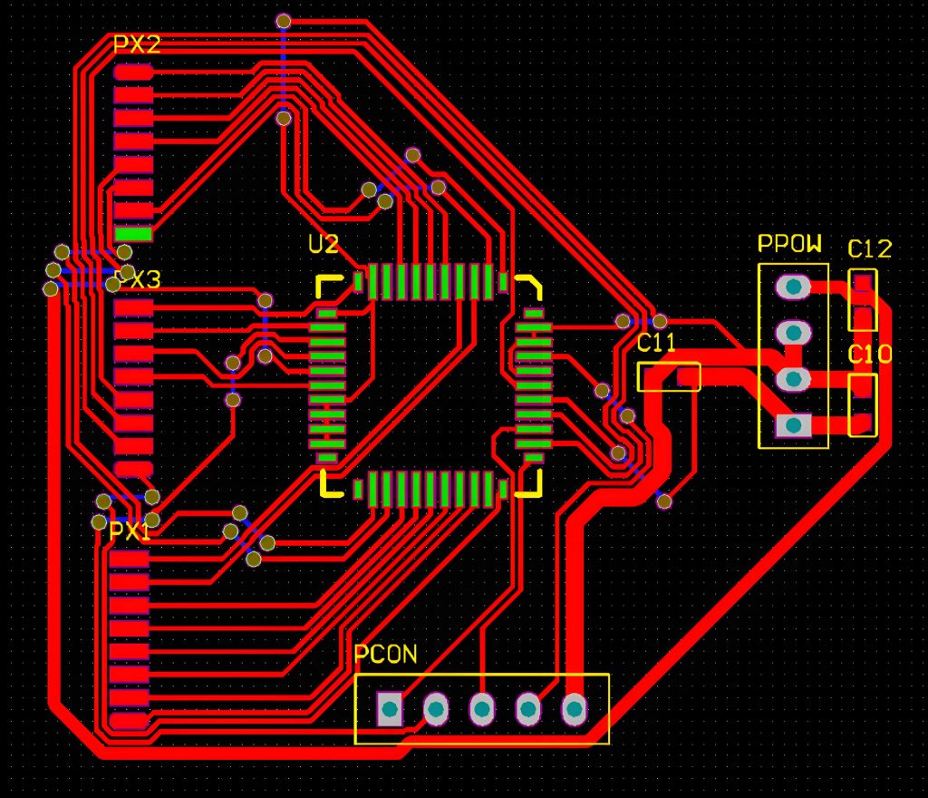
This method maintains uniform impedance, reduces reflection, and looks cleaner from the perspective of manufacturing.
4. Applying a solid and sustainable land field
Each signal requires a return path, and the path usually moves directly under the trail in the field of land. If the aircraft is damaged or has a cutout, the return path becomes longer and induces unwanted noise.
To fix it:
- Place a solid and uninterrupted land plane under a high -speed layer.
- Avoid the separation of aircraft across with high -speed signals.
- Minimize the transition of layers that force the return path to the detour.
The best technology uses special land aircraft and simulation validation to ensure that the return pathway is unbroken.
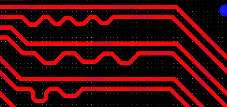
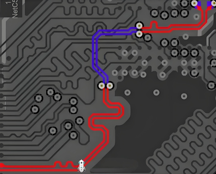
5. Length of differential pair matches
Differential pairs, such as USB, HDMI, or LVD lines, must be matched long to prevent signal slope. If one trail is longer than the other, time incompatibility can cause errors.
Some tips:
- Length matches in a few miles.
- Maintain a consistent distance (edge-to-tepi).
- Their route together, avoid various layers except really needed.
In the best technology, we support a suitable strict differential pair of up to ± 5 million during production.
6. Minimize the use of VIAS
Each Via adds capacitance and inductance, which reduces signal quality. High-speed signals do not like jumping between layers unless they are really needed.
If you have to use VIAS:
- Keep them short and consistent.
- Avoid unnecessary layer transitions.
- Use through stitches to maintain the continuous return path.
Our technical team is optimized through placement and offers VIAS blind and buried for complex HDI boards to reduce signal loss.
7. Use the right termination technique
Termination prevents reflection and stabilizes high -speed signals. Whether it’s a series, parallel, or termination of AC, it depends on the driver and your load settings.
For example:
- The termination of the series works well for point-to-point connections.
- Parallel termination helps in multi-drop settings.
Inappropriate ending can cause overshoot, ringing, or logic errors. We help customers in choosing the right termination resistor during DFM review.
8. Isolate analog and digital pages
Mixing analog and digital signals at risk. Digital circuits produce noise switching that can interfere with sensitive analog components.
Good layout practices include:
- Maintaining analog and digital circuits physically separate.
- Avoid crossover between analog and digital returns.
- Using the islands of the soil that is connected to one point if necessary.
Our layout reviews always evaluate signal isolation to avoid interference in the mixture signal board.
9. Differential Pair Route Together
Differential pairs must be diverted together, parallel, and in the same layer. If one signal deviates or loop, it creates an imbalance, which beats the benefits of differential signaling.
Also:
- Avoid lining them across separate planes.
- Keep them tight (consistent distance).
- Avoid fan-out unless required at the termination point.
Sophisticated PCB Manufacturing Equipment We keep a tight distance and alignment even at the interconnection of high density (HDI).
10. Observe the current return pathway
The high -speed return flow does not follow the shortest road € “they follow the least inductance, usually just below the trail.
Disturb the causes of the path:
- Loop ground
- Crosstalk
- Increased EMI
To prevent this:
- Avoid separation of fields across with signal traces.
- Use VIAS stitches to keep the return pathway close.
- Place the decoupling capacitor close to where the signal changes the layer.
We validate the return path during the layout verification using a signal integrity device.
11. Use stitching capacitors and soil VIAS
To suppress high frequency noise and EMI:
- Use a stitch capacitor between power and soil.
- Place the soil VIAS near the signal and connector transition.
- These components act like a firewall, maintaining noise from traveling on all boards.
We help customers determine the best placement for decouting and soil stitches to maintain signal purity.
Why trust the best technology for your high -speed PCB project?
In the best technology, we are specializing in manufacturing solutions and advanced PCB assembly, supporting industries such as automotive, aerospace, medical, and telecommunications. With ISO certification, we bring strict quality control for each project.
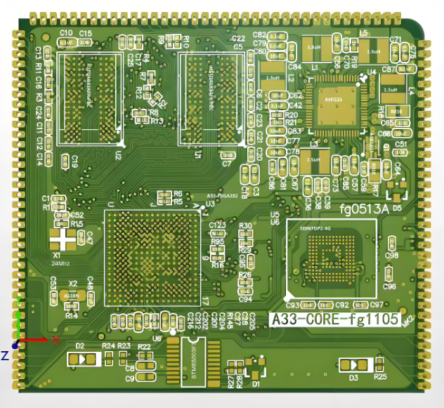
Since it was founded in 2006 as a printed circuit board manufacturer, the best technology has focused on high -quality, low to medium quality PCB fabrication, PCB assembly and electronic manufacturing. Our products and services include 1-40 print circuit board layers, thru-hole assembly, SMT assembly including BGA assembly, component sources, Turnkey box making and electronic product development. Whether you need a fast rotation prototype or volume production with controlled impedance, we are your reliable partners in high -speed design.
Want a reliable high -speed PCB? Contact the best technology today!
The high -speed PCB design is more than just a stomach, this is about understanding physics, signal behavior, and layout strategies. At the very least, we not only produce your boards, but also optimize it for real world performance.
Whether you need a HDI PCB, controlled impedance, a differential couple, or fast prototype, our team is ready to help.
👉 Let’s turn your next design into high -speed success. Contact us now to get a design offer or design consultation!
Frequently asked questions (FAQ)
1. What is considered a high -speed signal in PCB design?
Any signal with a rise/down time below 1NS or operating above 100MHz is considered high -speed, because it starts to behave like a transmission channel.
2. Can I use automatic routing for high -speed signals?
RUTO is automatically not recommended for high -speed nets. Manual routing provides better control over the length of traces, impedance, and matching.
3. What is leaning with differential pairs?
Skew refers to the postponement of time between two signals in the differential pair. The slope can cause data errors and must be minimized.
4. How do you calculate the impedance of the trail?
Traces impedance depends on the width of the trail, thickness, height of dielectric, and PCB material. Use online calculators or simulation tools such as polar or altium.
5. Can I run a high -speed signal on the outer layer?
It is better to retain high -speed signals in the internal layer between solid land plane to reduce EMI and maintain impedance.
This entry was posted on Tuesday, July 1, 2025 at 3:49 pm and submitted under the best PCB, BestTPCB, Design Guide, FAQ, FR4 PCB, PCB News. You can follow any response to this entry through RSS 2.0 bait. You can leave a response, or trackback from your own site.
Game Center
Game News
Review Film
Berita Olahraga
Lowongan Kerja
Berita Terkini
Berita Terbaru
Berita Teknologi
Seputar Teknologi
Berita Politik
Resep Masakan
Pendidikan
Berita Terkini
Berita Terkini
Berita Terkini
review anime
Gaming Center
Originally posted 2025-07-02 01:21:43.