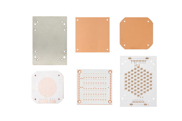
Heat is an invisible enemy of modern electronics. When the device is shrinking and soaring power density, efficient thermal management can not be negotiated. Metal -wrapped printed circuit board (MCPCB), using aluminum or copper base, is a labor for heat dissipation in applications such as high power LEDs, motor drive, and power supply. However, a critical factor but often ignored hiding in their layered structure: The thickness of the dielectric adhesive layer binds the circuit to the base of the metal. This thin film has great strength over your thermal performance. Let’s dissect why.
Core Problem: The adhesive layer is thermal resistance
The fundamental reason for the problem of adhesive thickness leads to physics: Thermal resistance. The heat produced by components (such as LEDs or mosfet) must be traveling through The adhesive layer to reach a very conductive metal base (substrate), which then spreads and disappears to the environment (through heatsinks, convection, etc.).
Adhesive material, even the thermal conductive one (often called Thermal interface materials – TIMS), has thermal conductivity (measured in W/MK) in size lower from copper traces or aluminum/copper base. For example:
- Aluminum: ~ 200 W/MK
- Copper: ~ 390 W/MK
- Typical thermal conductive adhesive: 1.0-4.0 W/MK (although some sophisticated formulations reach 8-10+ W/MK)
This adhesive layer is inherently the highest thermal resistance point in the primary heat path from the intersection of components to the main heat sink.
How thick is the thickness of strengthening thermal bottlenecks?
Thermal resistance (R_Th) of the adhesive layer itself is regulated by a simple but critical formula:
R_th_adhesive = l / (k * a)
Where:
- R_th_adhesive = thermal resistance of the adhesive layer (â ° C/W or K/W)
- L = thickness of the adhesive layer (meter)
- K = Thermal conductivity of adhesive material (W/MK)
- A = cross section area for heat flow (square meter)
This equation reveals the destroying impact of the thickness:
- Direct Proportionality (R_Th A L): Thermal resistance increases linearly with adhesive thickness. Duplicate thickness, double the thermal resistance. This is the most significant and direct effect. Thicker adhesive creates a longer heat path to travel through inappropriate material, significantly inhibits flow.
- Consequence: Higher component operating temperature (TJ), reduced efficiency, accelerated aging (depreciation of lumen in LEDs, shorter age), and potential reliability failure.
- Worsen low conductivity (R_Th A 1/K): While K is a material property, impact from low K is enlarged because the thickness increases. Poor adhesive (K = 1.0 W/MK) in the thickness of 100îiefm creates a much higher resistance than a good adhesive (K = 3.0 W/MK) in the same thickness. Making a thicker layer worsen the penalty because it uses low conductivity material. Optimize both of them K and L are very important.
- Increased interface resistance: The heat does not flow perfectly across the material boundary. Microscopic imperfections (roughness, cavity, worse) in the interface between components/circuits and adhesives, and between adhesive and metal base, for “contact resistance” additional. While mainly depends on the quality and surface pressure, a thicker The layer sometimes can make it more difficult to achieve optimal intimate contact in both interfaces simultaneously, potentially increasing effective Total interface resistance.
- Extended Heat Path: The thickness literally increases the heat energy that must be taken through conduction through resistive adhesive material before reaching a very conductive metal substrate. This longer pathway inherent slows down heat transfer.
Optimizing superior thermal performance
Achieve the best thermal performance requires a holistic approach that targets the thickness of adhesive, material nature, and manufacturing quality:
- Minimize thickness (L): This is a priority #1.
- Control Process: Apply strict process control during lamination (pressure, temperature, vacuum) to reach a consistent and ultra-thin bond line. Sophisticated techniques such as controlled flow adhesive and the right pressure profile is the key.
- Material Options: Choose adhesives specifically formulated for thin applications while maintaining the strength and reliability of dielectric. Some resin systems (for example, certain epoxy) inherent allows a thinner layer than the others.
- Target range: Struggle for the adhesive layer in the range 50îief to 100îief (2-4 miles) If possible, balance thermal performance with manufacturing and dielectric requirements. Going under 50 Us requires extraordinary process control.
- Maximize thermal conductivity (K):
- Filling Technology: The thermal conductive adhesive relies on ceramic fillers (Alâ‚oâ‚ion, Aln, BN, Sio “) in the polymer resin. Loading a higher filling increases K but has an impact on the viscosity and process ability. Look for formulations with optimal filling types, size distribution, and loading for maximum K.
- Further filling: Consider adhesive that uses higher performance fillers (although often more expensive) such as aluminum nitride (Aln) or boron nitride (BN) which offers a much higher intrinsic conductivity than standard alumina (alâ‚oâ ‘”).
- Verified data: D demand certified K value is measured using a standard method (for example, ASTM D5470), not just vendor claims.
- Optimizing the quality of the interface:
- Surface Preparation: Ensure excellent cleanliness and roughness/surface treatment that is appropriate on both sides of the circuit (usually copper) and the base of the metal before the lamination to promote the optimal wetting and adhesion.
- Void Elimination: Minimize the bubbles/void air trapped in adhesive or at the interface. Use the vacuum and adhesive laminate process with good flow characteristics.
- Uniformity: Achieve a very uniform adhesive thickness distribution throughout the board area. Locused thick spots are significant thermal traffic jams.
- Holistic Design & Synergy Material:
- Placement of components: Place the high heat -heated component directly above the base of the metal base with the best thermal connection (VIAS/minimum guttings underneath).
- Copper weight: Use a thicker copper layer (for example, 2oz, 3oz) on the circuit layer to spread the heat laterally before This enters adhesive, reducing the effective thermal gradient across adhesive.
- Metal basic choice: For extreme applications, consider the basis of copper (K is higher than aluminum) to further reduce the resistance of the spread of substrate after heat finally reaches that.
Designer checklist for thermal success:
- Determine the thickness of the adhesive: Don’t leave it as a reflection. Determine a maximum permitted The thickness requirements in your MCPCB specifications (for example, “The adhesive layer: Â ‰ ¤ 75 Us”).
- CERTIFIED D DEMAND K: Requires suppliers of adhesive or PCB manufacturers to provide reliable thermal conductivity data.
- Prioritize process skills: Choose a PCB manufacturer with proven expertise and strict process control for a thin, uniform adhesive layer. Ask about their lamination process, quality control steps (for example, ultrasonic scanning for cavities), and typical thickness consistency.
- Consider total thermal resistance (R_Th (JA)): In the end, evaluation all Thermal pathway from the intersection of components to ambient. While minimizing R_Th’s adhesive is very important, it also ensures an efficient heating heating outside the PCB.
Conclusion: thin inside (for thermal performance)
In high -risk game thermal management in a metal PCB, the thickness of the dielectric adhesive layer is not a small detail; This is the main performance dictator. Inherent thermal conductivity is low means that even a small increase in thickness dramatically increases thermal resistance, directly leads to hotter components and compromised reliability.
By understanding physics (r_th = l / (k * a)), focusing without stopping to minimize the thickness through sophisticated and manufacturing materials, maximize thermal conductivity, and ensure a perfect interface, engineers can unlock the potential for spreading heat from their metal substrate. Ignoring the thickness of the adhesive layer is a definite way to let the thermal problem quietly damage the performance and age of your product. Prioritizing thinness, prioritizing thermal conductivity, prioritizing the quality – your components will be grateful with cooler operations and longer life.
Tag: PCB is metal
This entry was posted on Tuesday, July 22, 2025 at 17:28 and was submitted under the best PCB, BestTPCB, FAQ, MCPCB, PCB Core Metal. You can follow any response to this entry through RSS 2.0 bait. You can leave a response, or trackback from your own site.
Game Center
Game News
Review Film
Berita Olahraga
Lowongan Kerja
Berita Terkini
Berita Terbaru
Berita Teknologi
Seputar Teknologi
Berita Politik
Resep Masakan
Pendidikan
Berita Terkini
Berita Terkini
Berita Terkini
review anime