If you need a two -sided copper PCB, are you curious?
What are the core benefits of two -sided copper PCB?
How much better the performance of the heat dissipation from a two -sided copper PCB than one side?
What complex design can be supported by two -sided copper PCB?
What application is PCB copper two sides suitable?
The best technology, professional copper PCB manufacturer, can answer your questions:
Two sides + double copper surface for heat dissipation increases the use of space and duplicating heat dissipation efficiency.
Double copper layer for conduction + very conductive base material with thermal resistance ≤0.6 ° C/W Increases the efficiency of heat dissipation by more than 40% compared to a single side PCB.
Fine line two side (width of lines/line lines ≥3 miles) Support through interconnection and copper that thickens locally.
High -power LEDs, power modules, automotive electronics, and other applications require high density cables and strong heat dissipation.
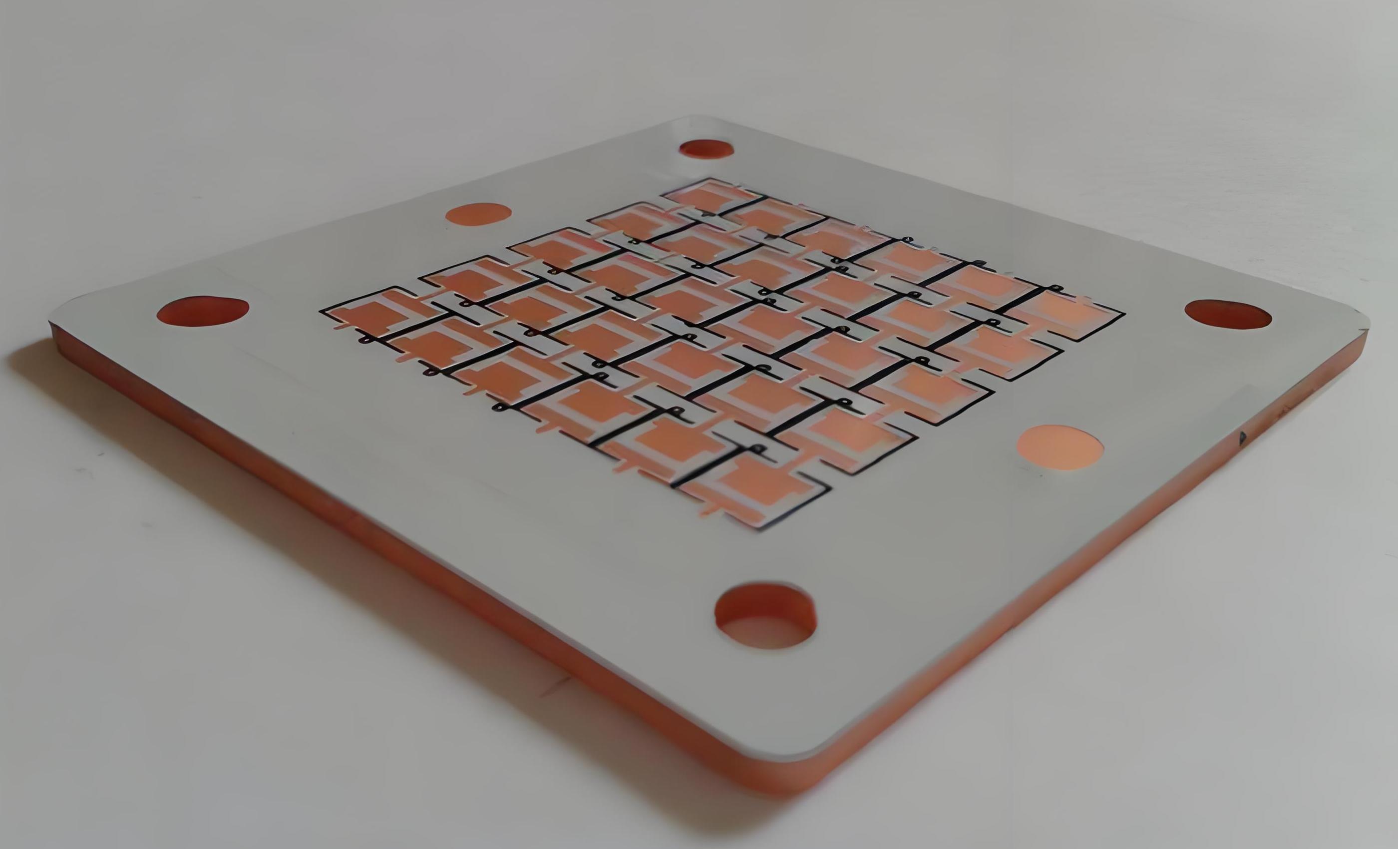
What is a double side copper substrate?
Two -sided copper substrate is type Metal core pcb It has a copper layer on both sides of the central core. The core is usually made of aluminum or copper, which gives excellent thermal strength and conductivity. This structure allows components to be installed and circuits to be diverted at the top and bottom, provide more design flexibility and improve performance.
Because the nucleus can spread heat quickly, this helps keep the components cold even under heavy loads. This makes it suitable for demanding applications such as LED lighting, power modules, automotive systems, and industrial control.
The ability to work on both sides allows more compact designs, reducing the size of the device without sacrificing functionality.
What is the difference between the single and double -side copper substrate?
The clearest difference is the number of copper layers and how the circuit is set.
- One -sided copper substrate: Copper is applied only on one side of the core. This is simpler, cheaper, and ideal for direct design with low component density.
- Two -sided copper substrate: Copper is applied to both sides, and covered in circuit circuits hole between them. This design supports a more complex stomach, higher power handling, and better thermal management.
The choice between them depends on the complexity of the product, size constraints, and performance requirements. If you need to package more functions into a smaller space while keeping the component cold, the two -sided option is a better choice.
What is the standard thickness of copper for copper substrate?
Copper thickness is one of the most important specifications for each substrate. General standards include:
- 1 ounce/ft² (around 35 μm): widely used for general electronics.
- 2 ounces/ft² (around 70 μm): For higher and higher thermal and thermal demands.
- 3 ounces or more: For heavy task force applications.
Thicker copper increases its current capacity and heat dissipation but can increase costs and weight. Thinner copper is lighter and cheaper but less capable of carrying high currents. Options must be made based on application requirements, balance performance and cost effectiveness.
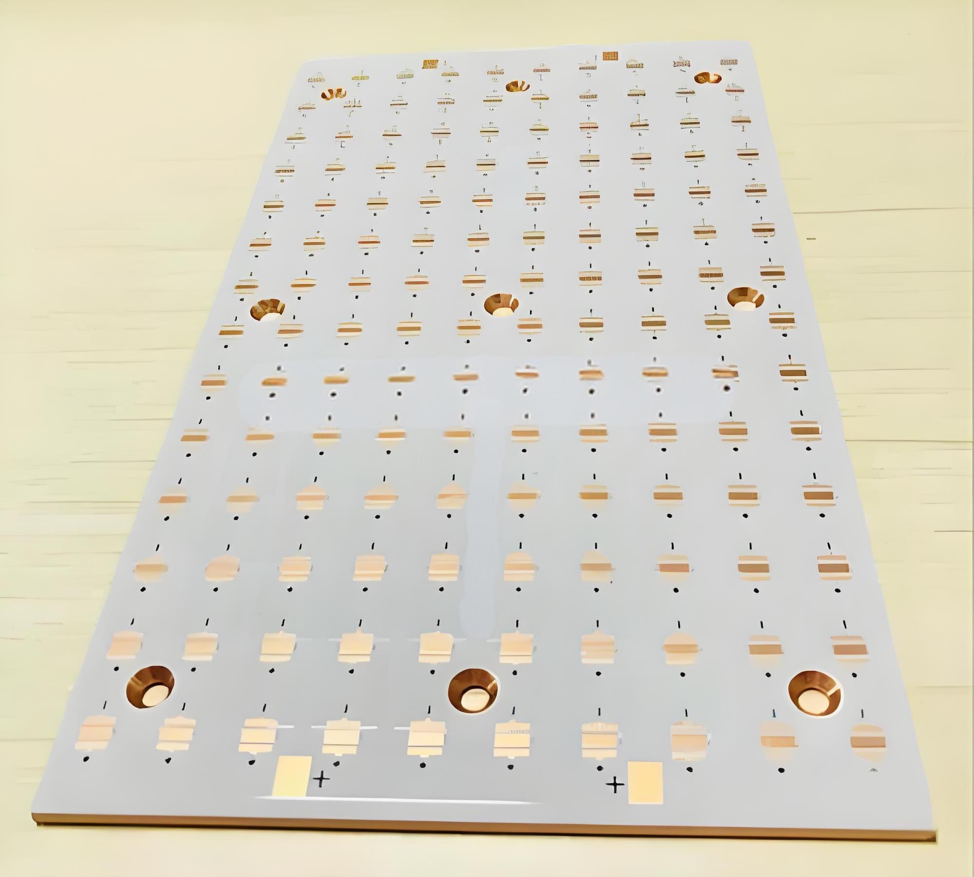
How thick is the two -sided copper substrate?
Total thickness depends on several layers:
- Metal core: Usually 1.0 mm to 3.2 mm.
- Copper layer: Usually each 35 μm to 105 μm each.
- Dielectric layer: 75 μm to 150 μm, thermal conductive but electric insulation.
Combined, a Two -sided copper substrate Often between 1.5 mm and 4.5 mm. A thinner board is ideal for compact devices, while thicker offers more strength and better heat management.
What are the advantages of the single side copper substrate?
Although the two -sided board is more advanced, one -sided copper substrate still has clear benefits:
- Lower production costs due to simpler manufacturing.
- Faster fabrication time line.
- Easier inspection and improvement because all traces are on one side.
- Good durability in a low demand environment.
- Perfect for applications where the complexity and heat output are low.
For basic products, this can be a smarter and more economical choice.
What are the weaknesses of the two -sided copper substrate?
The two -side board offers a lot of strength, but there are some limitations.
The price is more expensive to be produced because of additional copper layers, drilling, and coating process. Manufacturing time is also longer. Repair can be a challenge because the components are placed on both sides, making re -work more complex.
However, for high -performance products, this loss is often greater than a better circuit density, improvement of thermal performance, and expanded age. By choosing the best technology, this challenge can be handled effectively.
How do I do a two -sided copper substrate?
Manufacturing involves the right steps to ensure quality:
- Core Preparation: Clean and care for metal surfaces for adhesion.
- Dielectric lamination: Apply the thermal conductive layer, electric insulation to both sides.
- Copper Foil Bonds: Copper sheets for each dielectric under the heat and pressure.
- Drilling: Create a hole where the circuit requires a connection between sides.
- Plating: The interior hole layer with copper to form a conductive VIAS.
- Circuit pattern: Use Photolithography to determine the traces of the circuit.
- Etching: Remove the excess of copper, leaving only a designed path.
- Solder Mask Application: Protect copper from oxidation and short circuits.
- Surface finishing: Apply HASL, ENIG, or other final results for solderrability.
Each step requires accuracy, especially in drilling and coating, to guarantee the reliability of electricity.
What is the two -sided copper substrate on soldering?
The soldering method varies depending on the type of component:
- Solder reflow is common for the SMD component. The solder paste is applied, the part is placed, and the board is heated to melt the solder.
- Wave soldering Often used for components through the hole, passing the board above the liquid solder.
- Selective solder Used for boards that combine the surfaces of mount and through holes, targeting specific connections without affecting sensitive areas.
In all cases, hot control is very important to prevent damage to the dielectric or layered layer through a hole.
What connects the metal parts on the two -side copper substrate board?
The upper and lower copper layers are connected by layered through a hole (PTH). This is a drilling hole coated with copper to form a continuous electrical path.
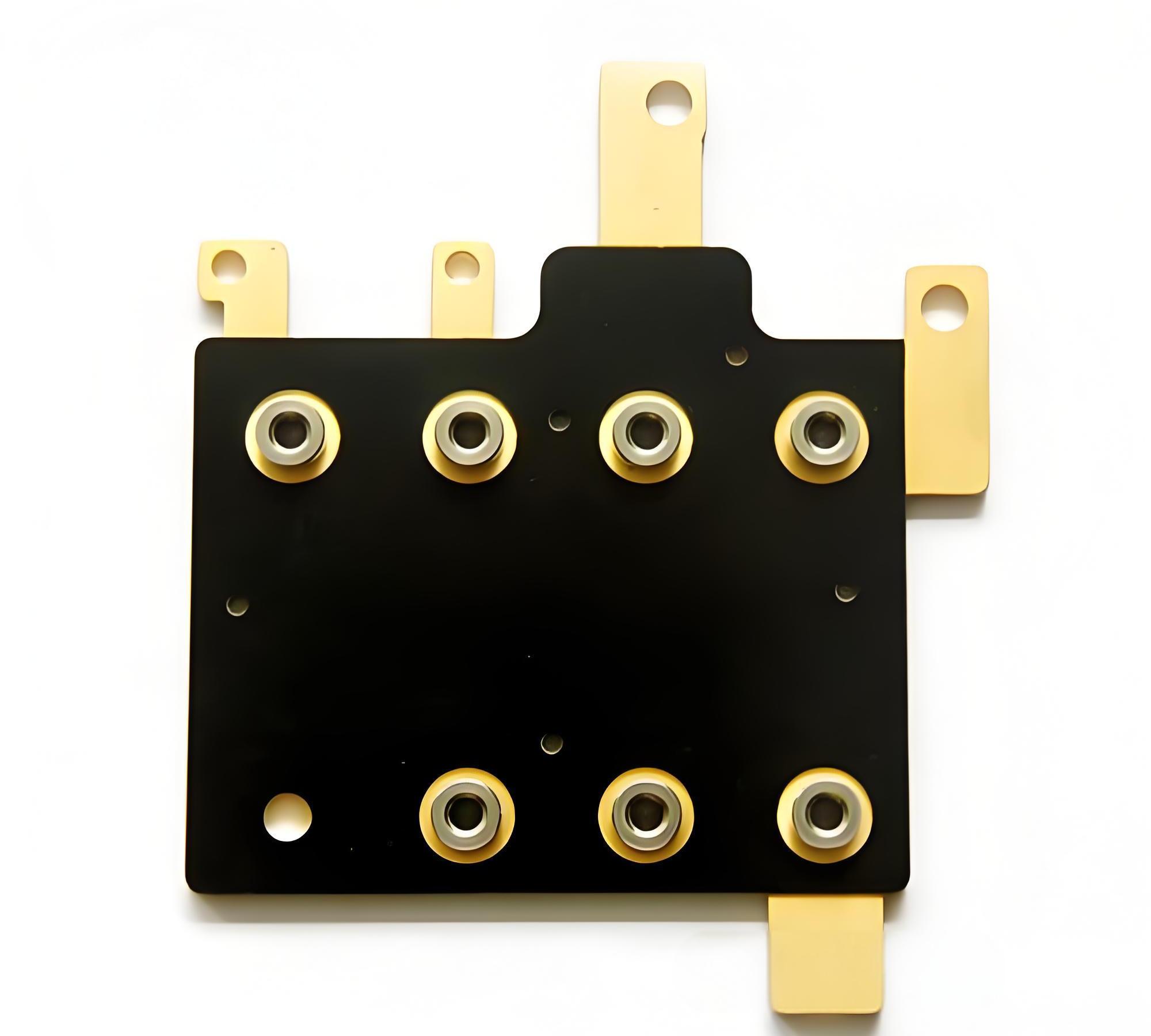
PTH carries a signal, supply power, and provides a foundation between the sides. In thermal design, thermal transfer heat from components to metal core for dissipation. High quality coating and proper drilling ensure that this connection can still be relied upon throughout the council’s life.
Conclusion:
Two -sided copper substrate Combining the strength of the metal core with the flexibility of two copper layers. This provides superior heat dissipation, higher circuit density, and better reliability for demanding applications. While more complex to be produced than one -sided board, the benefits make it an excellent choice for sophisticated electronics.
Contact: [email protected] for expert manufacturing support.
Tags: copper substrate, double side copper substrate, metal core PCB, metal core substrate
This entry was posted on Friday, August 15, 2025 at 17:53 and was submitted under the FAQ, MCPCB, Metal Core PCB, PCB Technology. You can follow any response to this entry through RSS 2.0 bait. You can leave a response, or trackback from your own site.
Game Center
Game News
Review Film
Berita Olahraga
Lowongan Kerja
Berita Terkini
Berita Terbaru
Berita Teknologi
Seputar Teknologi
Berita Politik
Resep Masakan
Pendidikan
Berita Terkini
Berita Terkini
Berita Terkini
review anime
Gaming Center
Originally posted 2025-08-17 19:41:26.