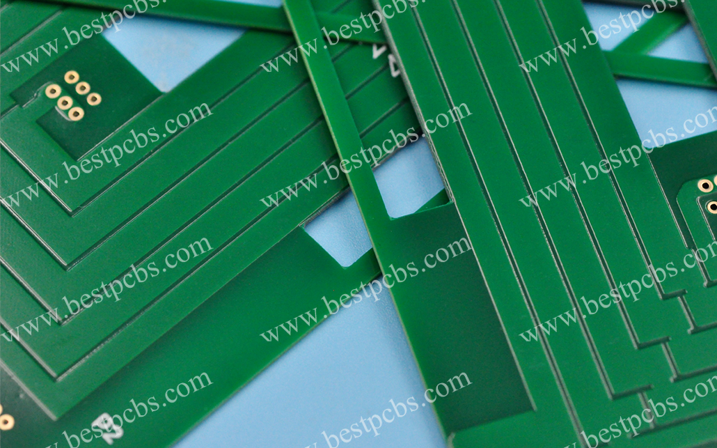
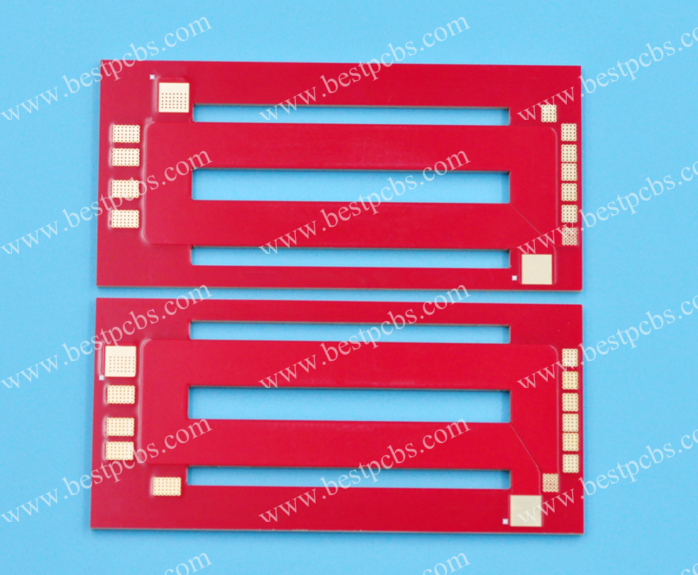
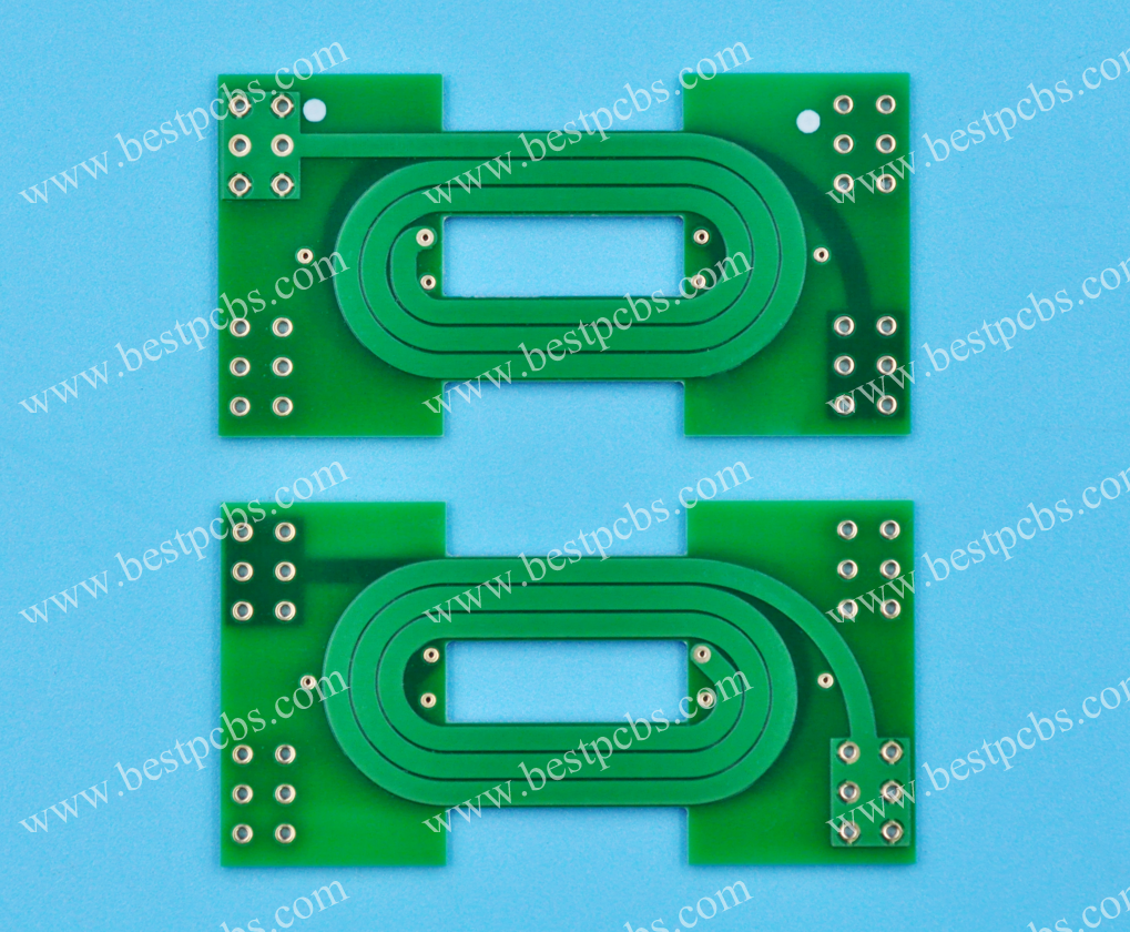
What PCB copper weight? Let’s explore the definitions, thickness conversion, current capacity, and selection criteria for PCB copper weight.
Are you having a problem with this problem?
Why does my high density PCB design continue to experience signal disorders?
How to balance the cost and reliability of PCB? Low -cost solutions are always unstable!
Small batch orders have a long waiting time. How can I quickly verify my design and prototype?
The best technology can provide services:
- Optimization of signal integrity: Use a simulation tool to predict disturbance and ensure the first EMC test.
- Cost Performance Balance: The selection of tiered copper thickness (1oz/2oz) saves 20% in material costs.
- Fast Prototype 48 Hours: A small batch production path specifically prioritizes urgent orders.
Welcome to contact us if you have a request for a heavy copper PCB: [email protected].
What is the weight of copper PCB?
PCB copper weight Referring to the mass of copper per square foot on the printed circuit board, measured in ONS (1 ounce = 28.35g). This directly has an impact on the current capacity, heat dissipation, and production costs, higher OZ values (for example, 2oz, 3oz) means thicker copper layer for heavy design, while lighter weight (1oz) is common in standard electronics. Engineers choose OZ values based on current requirements, thermal needs, and budget constraints, because thicker copper increases costs but increases endurance and performance.
What is the thickness of PCB copper?
The thickness of the copper pcb is the physical depth of the copper layer on the circuit board, measured in a microne (îief) or mile (1 million = 0.0254 mm). This defines how much current can be carried by traces, durability, and thermal performance. General thickness ranges from 0.5 ounces (17.5 î¼m) for high frequency design up to 4 ounces (140 î¼m) for high power applications. Thicker copper increases durability and heat dissipation but increases the cost and complexity of ETSA.
The difference between the copper weight of PCB vs thickness
| Attribute | Copper weight | Thickness |
| Definition | Copper mass per unit area (OZ/ft ² or g/m²) | Vertical height of copper layer (mile or î¼m) |
| Unit | ONS/square foot (oz/ft ²) or gram/square meter (g/m²) | MIL (MIL) or Micron (î¼m) |
| Direct relationship | Increased Copper Weight – Increased thickness (direct proportional) | Increased thickness of â † ‘increased gravity of copper (direct proportional) |
| Conversion formula | 1 oz/ft ‰ ‰ ˆ 34.8 î¼m (1,378 miles) | Thickness (î¼m) = copper weight (g / m²) / (8.96 Ã- 0.001) |
| Current impact capacity | Higher copper weight â † † ‘current power capacity is higher | Thicker thickness â † † ‘higher current capacity |
| Manufacturing impact | Requires the thickness of the suitable laminate and precision etc. | Requires controlled ETSA uniformity to avoid overcut/residue |
| Typical application | 0.5 oz/ft ² (17.5 îiefm) â † High density/BGA | 35 î¼m (1 oz/ft ²) â † ‘general signal layer |
| 2 ounces/ft ² (70 î¼m) â † ‘Package of strength/bad height | 105 î¼m (3 ounces/ft ²) â † ‘Industrial Control Board/RF |
Copper weight for thickness calculator
â € œDompper weighs to the thickness conversion ‘
- 1 ounce/ft ² = 1.37 miles (34.8 îiefm)
â € œICalculator formula ‘::
- Thickness (mils) = copper weight (oz/ft ²) × 1.37
- Thickness (î¼m) = copper weight (oz/ft ²) Ã – 34.8
Standard reference table
| Copper weight (oz/ft ²) | Thickness (î¼m) | Thickness (mile) |
| 0.5 | 17.4 | 0.685 |
| 1 | 34.8 | 1.37 |
| 2 | 69.6 | 2.74 |
| 3 | 104.4 | 4.11 |
| 4 | 139.2 | 5.48 |
How do you choose a PCB copper weight for high power applications?
Current capacity analysis
- Calculate the width of the trail required based on the max current using the IPC-2221 formula or an online calculator.
- Choose copper weight (1oz = 35â µm, 2oz = 70 μm) to match the width of the trace without exceeding the temperature rise limit.
Thermal management needs
- Use thicker copper (2oz+) for high power components (for example, power converters, LED drivers) to increase heat dissipation.
- Add the pour the thermal copper or VIAS under the heat component for additional cooling.
Consideration of signal integrity
- Prioritize thinner copper (0.5oz-1z) for high frequency circuits/RF to minimize loss of skin effects.
- Avoid excessive thickness of copper in a trail controlled by impedance.
Cost performance balance
- 1oz Copper is a standard for most consumer electronics (low cost, adequate for low/medium).
- 2oz+ reserves for industrial/automotive applications that require endurance.
Manufacturing constraints
- Confirm the ability of PCB FAB: thicker copper may require a special process (for example, coating, etching).
- Multi-layer boards with heavy copper can increase the waiting time and costs.
Mechanical power
- Use a heavier copper for PCB Flex/Rigid-Flex to increase the reliability of the bend.
- Thicker copper reduces the risk of track fracture under vibration or thermal cycle.
Compatibility of components
- The size of the pad matches the thickness of copper (for example, the SMT component requires a consistent solder connection).
- Heavy copper may require a greater VIAS/bearing for the right solder wetting.
Environmental factors
- Choose a heavier copper for the outside environment/high humidity to hold corrosion.
- Consider Enig/Enepig for heavy copper to improve solder capabilities.
The relationship between the current PCB vs. Copper Weight
Copper weight vs. current capacity
- Copper weight (oz/ft ²) directly determines the current carrier capacity. Thicker copper (eg.
- Practical Rules: 1 oz/ft ² copper â ‰ ˆ 1 a/mm of the width of the line (adjust to the increase in temperature and type of layer).
Track wide impact
A broader footprint reduces resistance and heat, allows higher currents. For example:
- 1 ounce/ft ² copper, width 0.25 mm ‰ ˆ 1.5 A
- 2 oz/ft ² copper, width 0.25 mm ‰ ˆ 2.5 A
- Use the IPC-221 or IPC-215 standard for the right calculation.
Constraints of temperature rise
- The permitted maximum temperature increase (for example, 10 ° C or 20 ° C) Determine the weight of copper and track width. Thicker copper reduces heat buildup in high -current applications.
Application Special Recommendations
- Low current (<1 a): Use 0.5â € “1 ounce/ft ² copper with a minimum track width. High current (> 3 a): Select 2â €” 6 oz/ft ² copper and broader traces (eg., ‰ ¥ 1 mm).
- Power Distribution: Thick copper (> 2 ounces/ft ²) is paired with the thermal Vias for heat dissipation.
Consideration of layers
- The external layer eliminates heat better than the internal layer. For internal traces, reduce the current capacity by 10â € “20% or use thicker copper.
Industrial Standards & Tools
- IPC-2152: Primary standard for current capacity, accounting for the type of layer, copper weight, and temperature.
- Saturn PCB Toolkit: Free software to calculate traces/through current capacity based on IPC-215.
Why choose the best technology as a PCB manufacturer?
- 19 Years of PCB Manufacturing Experience: Handling various problems encountered in PCB production flexibly and mostly reduce maintenance costs.
- ISO 14001/ISO 13485, Rohs/Reach Certification: Medical/automotive customers are exempt from secondary testing, and compliance costs are reduced by 30%
- Strict quality inspection: 1Quality inspection is 00% for bulk orders to reduce field failure.
- Fast turnaround (24-hour fast prototyping, mass production 5-7 days): Accelerated schedule without quality compromise.
- Cost -effective Solutions: Bulk discount and material optimization reduces PCB costs.
- Free DFM Analysis: Avoid expensive design, reduce the prototype iteration.
- Competitive price: Save 15â € “25% at PCB costs without reducing quality.
- Turnkey Solution: Complete PCB Manufacturing Services from Design to Shipping, Speed up the time-to-market of your product.
Contact the best technology to unlock cost savings, accelerated schedules, and flawless executions. Whether you need a fast prototype or high volume production, our team ensures the standard meets your PCB. Get offers now: [email protected].
Tags: PCB copper thickness, PCB copper weight, PCB copper weight vs thickness
This entry was posted on Tuesday, August 5, 2025 at 9:48 am and was submitted under the best PCB, BestTPCB, PCB Technology, Special PCB. You can follow any response to this entry through RSS 2.0 bait. You can leave a response, or trackback from your own site.
Game Center
Game News
Review Film
Berita Olahraga
Lowongan Kerja
Berita Terkini
Berita Terbaru
Berita Teknologi
Seputar Teknologi
Berita Politik
Resep Masakan
Pendidikan
Berita Terkini
Berita Terkini
Berita Terkini
review anime
Gaming Center
Originally posted 2025-08-05 05:45:17.