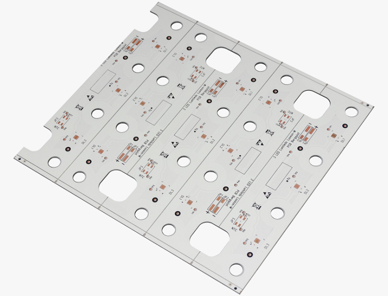
The structure of the IMS PCB plays an important role in modern LED applications, especially where thermal management is very important. LEDs produce heat during surgery, and poor heat dissipation can shorten their age. That’s where the IMS PCB enters € ”They manage heat effectively while maintaining electricity performance. Let’s explore the structure, benefits, and how to choose the right solution for your needs.
The best technology specializes in the IMS PCB, fabrication, assembly, and box building box prototype. Our factory is equipped with an automatic production line, and a general waiting time is shortened 5 days. And we support 48 hours of manufacturing prototypes. In addition, we provide an ideal solution from DFM analysis to fabrication. Doubts about the structure of the IMS PCB, don’t hesitate to tell us on [email protected].
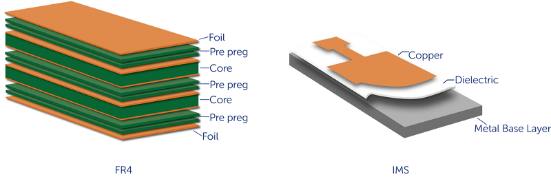
What is the structure of PCB STI?
STI is an abbreviation of isolated metal substrate, and its structure is designed to combine electricity performance with efficient heat dissipation. IMS PCB structure is built from three main layers:
- Copper foil layer The top layer forms a conductive circuit and carries an electrical signal with high reliability.
- Dielectric layer “The position is positioned between copper and metal base, this layer serves two vital roles: this provides electrical insulation and provides high thermal conductivity, usually starting from 1.5 to 8.0 W/M.
- Metal base layer “Usually made of aluminum or copper, this lower layer acts as a solid foundation and effective heat sink, spreading and removing heat from the board.
Together, these layers create structures that conduct electricity efficiently while also managing heat effectively, which is very important in LED and power electronic lighting. Unlike the FR4 board, the IMS PCB is built specifically for applications where thermal control is very important for performance and reliability.
What is the difference between the structure of the IMS circuit board and PCB FR4?
Let’s compare the IMS circuit board and PCB FR4 in terms of material and performance. PCB FR4 uses epoxy resins that are strengthened by fiberglass as a base, while the STI board uses a metal base. Insulation in STIs is thermal conductive but electric resistance. The comparison table here for better clarity:
| Feature | IMS circuit board | FR4 PCB |
|---|---|---|
| Basic material | Aluminum or copper | Fiberglass (FR4) |
| Thermal conductivity | Tall | Low |
| Durability | Stronger for hard use | Currently |
| Cost | Higher initial, lower long term | Lower initials |
Obviously, the IMS PCB structure offers better thermal performance, which is the key to LEDs that must run cool and stable.
How long is the STI circuit board in a hard environment compared to FR4 PCB?
Durability is the main concern for LED applications in external or industrial settings. IMS PCB handles extreme temperatures, humidity, and mechanical stress better than the FR4 board. The metal base provides strength and stability, while isolation rejects damage. As a result, the IMS circuit board lasts longer and requires less replacement, reducing maintenance costs. Many customers face the initial LED failure because of the poor PCB resistance ”IMS technology solves this problem efficiently.
How do you choose the right isolated metal substrate for your PCB structure of your STI?
Choosing the right metal substrate depends on your specific needs. For standard LEDs, aluminum is common. For higher thermal demand, copper may be better. Also, consider the basic thickness of metal and dielectric layers. Thicker metals can handle more heat but add weight and cost. This is a Short Guide:
- Aluminum:Affordable, good for most of the use of LEDs.
- Copper:Higher thermal performance, higher costs.
- Dielectric layer:Select based on thermal resistance (lower better).
Working with experienced PCB IMS Manufacturers can help you make the right choice without waste time or money.
What is the process of making a PCB of STI Board?
Producing the PCB IMS board involves several right steps to ensure thermal and electric performance. This is the way the process works:
- Material selection
The process begins with choosing the right metal base ‘”usually aluminum or copper” based on thermal and mechanical needs. - Metal basic preparation
The metal base is thoroughly cleaned to remove contaminants. This ensures strong adhesion and consistent quality in the next layer. - Dielectric layer application
Dielectric layer Thermal conductivity is high laminated to the base of the metal. This layer provides insulation and helps transfer heat efficiently. - Copper foil lamination
The copper foil is then bound to the top of the dielectric layer. This copper layer will form a conductive circuit path. - Circuit pattern
Using photoresis and chemical etc., the desired circuit design is made on copper surfaces. This step must be appropriate to avoid defects. - Drilling
Hole for the placement of components or VIAS is drilled using automatic equipment for accuracy and consistency. - Finishing surface
Surface finishing such as Enig, OSP, or Hasl is applied to protect copper and increase solder capabilities. - Quality testing and control
Each board undergoes electricity testing and thermal performance checks. Damaged boards are removed to maintain high standards.
The best technology controls every stage with care -heart. As a professional IMS PCB manufacturer, the best technology gains special knowledge in the MCPCB industry, and we have a stable and up -to -date manufacturing process and strict quality control. Every question about the selection of material, the structure of the STI PCB, or any assistance with the PCB IMS project, please tell us at [email protected].
What is the value of the IMS PCB structure for LED?
The structure of the IMS PCB provides a significant value in LED applications, especially where heat and reliability discipline is very important. Many customers experience LED failures due to poor thermal design, which causes reduced brightness, shorter product life, and expensive replacement. PCB IMS discusses this problem effectively. This is how:
- Superior heat dissipation
The most important value of the IMS PCB structure is its ability to heat up from the LED intersection efficiently. A metal base combined with high dielectric conductivity (1.5â € “8.0 w/m) ensures heat is spread and released quickly. This prevents thermal buildup and makes LEDs operate at safe temperatures. - Longer life
Overheating is the main cause of LED failure. By maintaining low temperatures, the STI board helps extend the LED surgery period. This reduces the need for maintenance and frequency of replacement, especially in the outside or industrial environment. - Stable light output
Temperature affects LED brightness and color stability. IMS PCB structure helps maintain consistent light output over time, which is very important for lighting applications in the retail, automotive, or architecture sectors. - Concise and lightweight design
Because the STI board handles heat very well, designers can reduce the size of the heat sink or eliminate it completely. This allows LED products that are slimmer and lighter without reducing performance. - Cost efficiency from time to time
While PCB IMS may have a higher initial cost than FR4, they offer long -term savings by reducing failure rates and minimizing heat -related damage. For high power LED systems, STIs are cost -effective solutions. - Greater reliability in a hard condition
LEDs used in outdoor lighting, automotive, or factory settings must withstand vibrations, humidity, and changes in temperature. PCB IMS provides mechanical strength and thermal stability, making it very reliable in a difficult environment. - Fewer failure, higher customer satisfaction
Poor thermal designs often lead to customer complaints and product returns. IMS technology helps companies provide long -lasting and high -performance LED products, increase customer confidence and reduce warranty claims.
In short, the structure of the IMS PCB adds value by increasing heat control, product durability, and design flexibility. For any LED application where efficiency and reliability, STIs are an intelligent and ready choice in the future.
Why choose the best technology as your Chinese IMS PCB manufacturer?
The best technology understands your concern ”slow delivery, poor quality, and unclear communication. We resolve this headache through the following strength:
| Customer pain point | Best Technology Solution |
|---|---|
| Delivery is delayed | Fast prototype and strict waiting time management |
| Low quality | Certified by ISO 9001, ISO 13485, IATF 16949, AS9100D, UL, Rohs; Full quality examination |
| Unstable supply chain | Traceity with a mes system and reliable source |
| Technical support gap | Professional Engineers Ready for Design Suggestions |
With 19 years of experience, strict quality control, and responsive service, the best technology is the right partner for your PCB STI needs. From LED lighting to industrial control, we provide quality that you can rely on. For PCB IMS questions from prototype to assembly, please tell us [email protected].
Tag: IMS PCB Structure
This entry was posted on Monday, July 28, 2025 at 18:20 and was submitted under the best PCB, BestTPCB, MCPCB, SinkPad. You can follow any response to this entry through RSS 2.0 bait. You can leave a response, or trackback from your own site.
Game Center
Game News
Review Film
Berita Olahraga
Lowongan Kerja
Berita Terkini
Berita Terbaru
Berita Teknologi
Seputar Teknologi
Berita Politik
Resep Masakan
Pendidikan
Berita Terkini
Berita Terkini
Berita Terkini
review anime