Copper Inlay PCB is a special circuit design method that significantly increases the ability of heat dissipation and current loading performance by entering copper in PCB. This technology is widely used in power electronics, car electronics, and devices, bro, helps overcome the difficult heat management problems of traditional PCBs in high -empowered environment and high density.
Do you suffer from this headache?
- Poor heat dissipation problems on traditional PCB?
- High manufacturing difficulties and cost problems, such as easy to have the problem of alignment and material waste?
- The problem of compatibility between design and manufacturing? For example, in the design, there may be a compatibility problem between the inlay copper structure and other parts of the PCB, such as alignment of layers, hole diameter, and edge care, which ultimately causes increasing manufacturing difficulties.
- Problems with the selection of material and costs?
Here are some of the real solutions to use the best technology in customer projects.
- Optimizing the design and manufacturing process: The best technology adopts high precision manufacturing processes, such as laser or photolitography.
- Optimizing material selection: We use copper material with high purity to increase conductivity and mechanical performance. In addition, select a copper substrate or aluminum substrate to improve the performance and reliability of thermal discipline.
- Control the costs and increase manufacturing: The best technology optimizes design to reduce material waste and manufacturing complexity.
- Optimizing heat dissipation and thermal management: We use the Multilayer copper inlay structure to improve thermal dissipation capabilities
The best technology provides copper PCB design optimization, prototype, mass production, and assembly services. We have a productive experience to overcome the problem of thermal discipline, manufacturing difficulties, and material selection problems. If you have technical questions or doubts, a warm welcome to contact us at [email protected].
What is Copper Inlay PCB?
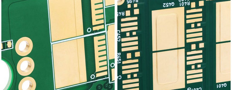
Copper Inlay PCB integrates solid copper pieces into the PCB specific area. This is useful to improve the ability of conductivity and rapid heat dissipation performance. In high or high current applications, this design is more reliable than a pure design makes a thicker copper layer.
What is the connection: the thickness of the copper layer in the PCB, the PCB inlay copper?
Copper thickness in the PCB directly affects the electrical and thermal behavior of the board. It is good to know that if pure depends on the thickness of copper can not meet the demands in high power applications, then copper inlay PCB has a key role here. This increases the thickness and quality of copper in the area, so that it can improve current load performance and heat dissipation.
| Aspect | PCB Inner Layer Copper Thilmness | Copper pcb inlay |
| Definition | Standard copper thickness used in all layers of PCB | Solid copper block embedded in the selective PCB area |
| Main role | Supports the flow of currents and basic thermal paths | Handling high -current and local heat dissipation |
| Application | General PCB Design, Balanced Power Distribution | High strength zone, high density, or thermal stress |
| Performance impact | Limited by the thickness of copper as a whole | Significantly increase the ability of current and thermal |
What’s the difference: PCB inlay copper, pour copper on the PCB?
Copper and copper inlay is a different strategy. Pour copper on a PCB generally for earthing a large area or power distribution; However, copper inlay PCB is to strengthen the area area. The first is limited to the thickness of copper, and its heat dissipation capability is limited. However, the latter of direct heat through solid copper blocks, and the effect is more significant.
| Aspect | Copper pcb inlay | Pour copper on PCB |
| Material | Solid copper blocks are put into the PCB cavity | Large copper area formed by coating during the PCB process |
| Objective | Local thermal controls and high current paths | Power aircraft, land aircraft, signal return paths |
| Precision | Highly targeted in certain PCB zones | Scattered on the broad section of the board |
| Thermal efficiency | Superior, because of direct copper mass and conduction | Limited by copper thickness and field size |
Why does PCB use copper inlay?
PCB uses copper inlay to overcome the problem of heat dissipation bottleneck and the excess of current charge. Because the device gets smaller and smaller when the power is bigger and bigger, the traditional PCB copper layer is easily heated, which causes failure. Copper Inlay technology provides stable thermal paths and current routes, which reduce the rate of failure and extend the life of the product radically.
How do I put copper into the PCB?
- The fabrication process includes cutting copper blocks → put it in the PCB cavity → Lamination bonds → general drilling, coating, and etching processes.
In this way, it not only ensures the bond between copper blocks and circuit boards but also ensures the smoothness of the surface and the effect of the overall heat conductivity. In actual production, it may be necessary to adjust the process according to specific parameters, such as the thickness of the copper block and the substrate type.
What is the price of copper PCB Inlay?
The price of copper PCB inlay depends on the size of the board, the complexity of the design, and the quantity of copper blocks. Although the cost is higher than the general PCB, in high power applications, it will reduce improvement and maintenance Cost significantly due to good heat dissipation. Therefore, of all age costs, it will be more cost effective.
What are the advantages of the thermal device bro with copper PCB inlay in high power applications?
The thermal Gan device with the PCB copper inlay gives engineers to manage extreme heat and high currents. And that is the center of attention in high power applications.
- High efficiency of heat conductivity on PCB minimizes the risk of devices that are too hot, supporting consistent performance and even in demanding conditions.
- Increased heat management ensures high frequency operations that are more stable and improve switching performance, make the device suitable for strict tasks.
- Copper PCB Inlay allows devices to handle higher current density without losing performance or overheating.
- Maintain reliable operations in compact design.
- Expand the age of the device and reduce heat pressure.
How does PCB copper inlay increase heat dissipation?
Inlay copper PCB offers direct heat dissipation pathway for the main heating component. Specific performance is as follows:
- Do the heat quickly to the copper layer or heat sink.
- Reduce the operating temperature of the main component.
- Reduce hotspots and protect sensitive devices.
- Increase the efficiency and stability of integrated power.
- Extend the operation of the age of the circuit board.
In short, copper PCB inlay is a solution that can be applied to overcome problems in heat discipline from high -powerful and high -heat applications, and in electricity performance. The best technology wins customer trust and repetition because our team not only ensures customers get reliable and high -performance circuit boards through our strict quality control and fast waiting time, but also provide high quality solutions. If you have a new project, don’t hesitate to contact us for free DFM analysis, fast prototype, full turnkey fabrication, assembly, and box making services at [email protected].
Tag: copper pcb inlay
This entry was posted on Thursday, August 21, 2025 at 18:36 and submitted under the best PCB, BestTPCB. You can follow any response to this entry through RSS 2.0 bait. You can jump to the end and leave a response. Pinging is currently not permitted.
Game Center
Game News
Review Film
Berita Olahraga
Lowongan Kerja
Berita Terkini
Berita Terbaru
Berita Teknologi
Seputar Teknologi
Berita Politik
Resep Masakan
Pendidikan
Berita Terkini
Berita Terkini
Berita Terkini
review anime