How to design copper pcb plates? This guide includes substrate specifications, design guidelines, thermal solutions. The manufacturing process for copper PCB plates.
- Does your 5G base station power device experience performance degradation due to insufficient heat dissipation?
- PCB new energy vehicles are delaced in high temperature conditions. How do you penetrate the traffic jam of reliability?
- In a high -current carrier scenario, does the thermal expansion coefficient of the traditional FR4 substrate affect the life life?
The best technology can provide:
- Custom copper substrate through a combination ‰ ¥ 2oz copper thickness + dielectric layer of ceramic charging, thermal conductivity increases to 400w/mk, ensuring that the increase in temperature of high power devices is reduced by 30%.
- CTE matching technology using copper/aluminum composite substrate, the thermal expansion coefficient is very suitable with semiconductor devices to avoid high temperature delamination risk.
- Modular Thermal Management Design – Integrated and optimized heat pipes are optimized through arrays to achieve stable operations at 15A/mm² current density.
Welcome to contact us if you have a request for copper PCB: [email protected].
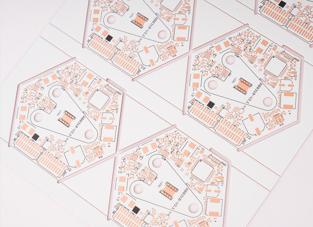
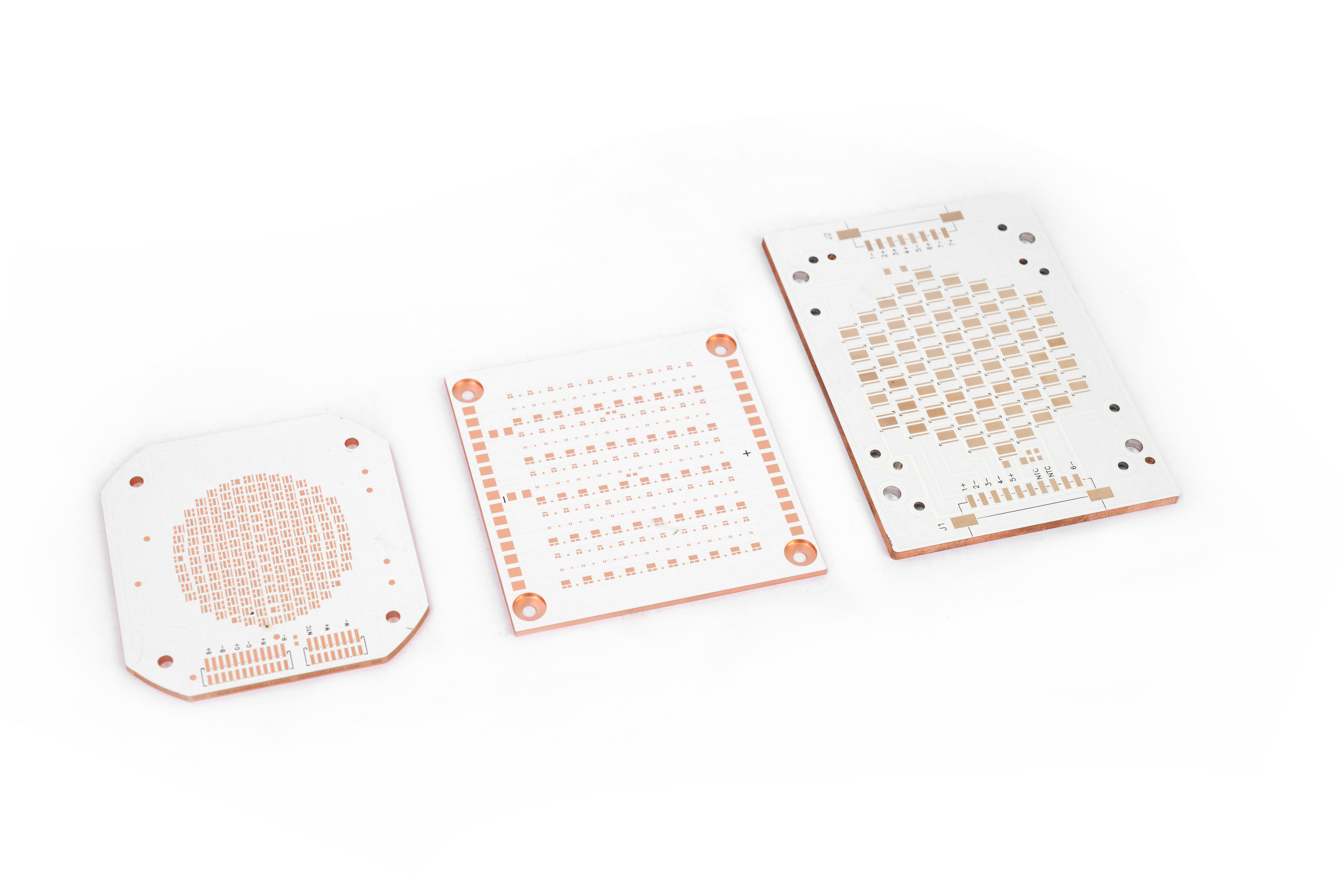
What is a copper PCB plate?
A copper pcb plates is a printed circuit board using solid copper as the main substrate material. This design is basically replacing standard insulation substrates such as FR-4 with solid copper core, functioning simultaneously as a structural circuit foundation and primary heat dissipation media.
The dielectric isolation layer of construction and conductive copper foil directly into the copper base. This integration utilizes the thermal conductivity attached to copper to absorb and transfer heat from electronic components, establish an efficient thermal path while maintaining electrical insulation.
Copper Substrate PCB Specifications
| Parameter | Specifications range |
| Copper thickness | Standard: 1oz (35î¼m), 2oz (70 Us) ï½ œheavy: 3oz (105îief) -10oz (350îief |
| Substrate thickness | 0.2mm-3.2mm (typical aluminum core 1.0mm/1.5mm/2.0mm) |
| Thermal conductivity | 1-8W/(mâ · k) (typical aluminum core 2-3w) |
| Dielectric strength | AC 1KV-4KV (2.5KV@1mm substrate spacing) |
| Max panel size | Single/Double-Side: 800ã-1200mm ½œ Multilayer: 610ã-1100mm |
| Copper type | Rolled (High Dactility) |ectrodeposited (Standard) |
| Final surface | HASL (LF), ENIG, OSP, IMMERSION AG (ENIG is preferred for impedance control) |
| Min trace/space | 1Oz: 4/4mil|3oz: 8/12mil (IPC-2152 Required current carrying capacity) |
Copper pcb plate application
- Automotive ‘ – EV battery management, motor controller, charging system.
- Telecommunications’ – 5G/6G base station, RF power amplifier, antenna module.
- Industryâ € œ – Welding machine, UPS, Solar Inverter, Robotics.
- Aerospace ‘ – Satellite Comms, Avionics, Radar Systems.
- Medical ‘ -MRI equipment, surgical laser, X-ray generator.
- Consumers’ -Smartphone high class, game console, AR/VR device.
Copper PCB Plate Design Guidelines
1. Election & thickness of material
- Use the thickness of the copper foil based on the current requirements: 1oz (35 Us) for standard applications, 2oz (70îief) or thicker for high current design.
- The thickness of the inner layer ‰ ¥ 0.5oz; The outer layer adds 0.5oz to the base thickness.
- Make sure the thickness of the dielectric layer ‰ ¥ 0.1mm to prevent voltage damage.
2. Layout & Stackup layer
- Symmetrical design adoption for dielectric layers, copper thickness, and trace distribution.
- Separate high -speed/low -speed aircraft, digital/analog, and power/ground using spatial isolation or special base lines.
- Place high power components centrally even for heat distribution; Avoid grouping.
3. Thermal management
- Increase the copper area under the high power device to act as a heat spreader.
- Use the thermal Vias to connect the top/bottom layer, transfer heat to a special thermal bearing.
- For current> 10a, select ‰ ¥ 2oz copper and widen to reduce resistance.
4. Signal integrity
- Maintain rule 3W (traces of spaces ‰ ¥ 3ã – trace width) to minimize crosstalk.
- The high -speed signal route (for example, the clock channel) away from the noisy electric channel.
- Make sure the impedance control for differential pairs and critical nets.
5. Manufacturing considerations
- Follow IPC-2221 for a width/distance trail and IPC-6012 for quality class (class 3 for aerospace/medical).
- Avoid sharp angles (> 135 °) to prevent EMI and manufacturing defects.
- Use a solid copper or hatch with permission â ‰ ¥ 0.2mm from the bearing/VIAS.
6. Power & Land Design
- Dedicated separate fields/land for the analog/digital section.
- Disseminate power traces and use several VIAS for low impedance pathways.
- Applying a local decoupling capacitor near ICS (‰ ¤0.3mm from an electric pin).
7. Drilling & Coating Design
- For thick copper (> 4oz), optimize drill parameters to reduce copper and grinding stains.
- Make sure the thickness of the hole wall coating ‰ ¥ 25îiefm for the reliability of class 3.
8. Testing & Validation
- Perform thermal imaging to validate heat dissipation in the high power zone.
- Use impedance tests for high -speed signals and electrical continuity checks.
- This guideline balances performance, manufacturing, and reliability while complying with industrial standards.
The thermal solution of copper pcb plates in electric vehicles
Five thermal solutions for Copper pcb plates in an electric vehicle
1. High conductivity substrate & thick copper layer
- Use Metal pcb (Mcpcb) or ceramic substrate (alâ ‘ƒ “/aln) with thermal conductivity> 1.5 W/Mâ · K for the power module.
- Apply a thick copper of localized (‰ ¥ 2oz/70 Us) to a high -current trail to reduce joules and increase heat spread.
2. Thermal solid through arrays under high power components
- Place the thermal Vias (0.3 € “diameter 0.5mm, 1.0mm pitch) just below IGBT, Mosfet, or DC-Link capacitor.
- The contents of VIAS with copper or conductive paste to remove air gaps and increase vertical heat transfer.
3. Optimization of Zoning & Component Placement
- The center of the heat -producing device near the liquid coolant or heat sink.
- Maintain a distance of ¥ ¥ 5mm between high voltage (> 600V) and low voltage circuits to prevent thermal crosstalk.
4. Hybrid cooling integration
- Combine the thermal VIAS PCB with active cooling (for example, microcnel fluid cooling plates) for modules that exceed 200W.
- Use the Change Material Phase (PCMS) or graphite sheet between PCB and housing for passive thermal buffering.
5. Simulation -based design validation & automotive class
- Perform CFD thermal modeling (for example, ANSYS ICepak) to optimize through density and material selection.
- Validation through power cycling tests (200a, 1000+ cycles) and thermal shocks (-40 ° C to + 150 ° C) per standard AEC-Q100.
How is the copper base PCB made?
Production process Copper base pcb:
1. Material selection ‘: Starting with 99.9% of pure copper plates (thickness 1-10mm) and the thermal conductive dielectric layer (usually aluminum nitride or polymer filled with ceramics).
2. Surface maintenance ‘: Chemical clean copper surface to achieve roughness <0.5îief, then apply oxidation resistant layer for better bonds.
3. Transfer pattern ‘:: The lamination of the dry film Phoresist to copper, describe with UV light through the work of art designed, then develop to make a circuit pattern.
4. Etsa precision ‘:: Use the ammonia ETSA solution that is maintained at 45 ± 2 ° C to eliminate unwanted copper, reaching the tolerance of the 50îlen line width.
5. Dielectric bonds’:: The thermal conductive dielectric sandwich between the copper layer below 180 ° C and 15kg/cm ² pressure for 90 minutes.
6. Drilling & Coating â € œ: Micro-Via drill with a diameter of 0.1-0.3mm using a laser ablation, then an electric copper plate.
7. Soldder Mask Application ‘: High-temperature-print-print-resistant ink screen (hold 260 ° C for 60s), heal with infrared to improve thermal cycling performance.
8. Surface finishing ‘: Apply Enig (Electric Nickel Soaking Gold) or Silver Coating for Optimal Sutderability and Heat Discussion.
9. Electric testing ‘:: Perform a 100% continuity test with 500V DC and measurement of thermal impedance using the ASTM D5470 standard.
10. Final Inspection “: Dimensional accuracy verification (± ± 0.05mm) and thermal conductivity (range 300-500W/MK) before vacuum packaging.
Reliability compliance testing for copper pcb
1. Validation of thermal cycling resistance ‘
- Run 1,000 fast temperature cycles between -55 ° C and +150 ° C after IPC -9701. Confirmation of thermal conductivity that is maintained in deviation of ± 5% to ensure long -term stability in automotive applications.
2. Dielectric resistant voltage test ‘
- Apply 3.5kv AC for 60 seconds between adjacent copper layers per UL 94V-0. Stop the test if the leakage current exceeds 10mma, guarantees the integrity of isolation in a high voltage design.
3. Assessment of thermal shock resistance ‘
- The transition board between -65 ° C and +175 ° C in the room in 10 seconds per jedec jesd22 -a106b. Check the delamination after 300 cycles using acoustic microscope scanning.
4. Solder Reflow Compatibility Check ‘
- Soak test coupon in the Solder 288 ° C for 30 seconds (IPC-TM-650 2.6.8). Verification of dimensional changes <0,2% dan kekuatan adhesi mask solder> 1.0kgf/cm ² post-test.
5. Evaluation of humidity aging ‘
- Sample condition at 85 ° C/85% RH for 168 hours (JESD22-A101). Measure Isolation Resistance> 100mî © After recovery to show reliability in the tropical climate.
6. Mechanical flexural strength test ‘
- Perform bending three points at 150 ° C with a strain of 0.5% (IPC-6012). Validation of zero microcracks through cross -sectional analysis to ensure structural robustness.
7. Measurement of the strength of the interlayer bonds’
- Perform skin tests 90 ° before/after thermal aging (IPC-TM-650 2.4.8). Maintain> Adhesion Strength 1.2kgf/cm for the power module application.
8. VERIFICATION OF HIGH LOOKING
- The subject board for 100A DC loads at 110 ° C is around 24 hours (IEC 60146). Monitor thermal increase <40 ° C above ambient with infrared thermography.
Why choose the best technology as a producer of copper PCB plate?
- DFM Analysis (Design for Production) Free: Optimizing the PCB layout to reduce material waste, lower production costs, and avoid the final design revision.
- Thermal Simulation & Optimization: Special heat dissipation solution is proven to reduce the temperature of the hotspot by 25-40 ° C
- Fast Prototype Delivery 24 Hours: Speed up the product development cycle, allowing faster time to the market and competitive advantage in the high demand industry.
- Strict quality control with 100%inspection: Eliminating hidden defects, reducing re -work costs, and ensuring reliability in high/thermal application.
- Transparent prices without hidden costs: Predicted budgeting and cost savings through the face setting model that is tailored to the specifications of the thick copper PCB.
- Certified Compliance (ISO 9001, UL, Rohs): Reducing regulatory risk and ensuring products meet global standards for environmental safety and compliance.
- One -roof solution from design to shipping: Streamline project management by consolidating prototypes, fabrication, and joint assembly.
Welcome to contact us if you have questions for copper PCB boards: [email protected]. See you hear from you soon!
Tag: copper base pcb, copper pcb plate
This entry is posted on æÿœœä º “, 18 7 æœatra, 2025 at 3:53 ¸‹ Å ˆ and submitted under the best PCB, BestTPCB, MCPCB, PCB Core Metal. You can follow any responses to this entry via RSS 2.0 feed. You can leave a response, or trackback from your own site.
Game Center
Game News
Review Film
Berita Olahraga
Lowongan Kerja
Berita Terkini
Berita Terbaru
Berita Teknologi
Seputar Teknologi
Berita Politik
Resep Masakan
Pendidikan
Berita Terkini
Berita Terkini
Berita Terkini
review anime