What Copper Coating PCB? Let’s find the meaning, benefits, applications, methods of coating and process through this blog.
Are you worried about this problem?
- How to solve the problem of uniformity of thick copper plate layers?
- How do you control the coating defect in the copper deposition process?
- Can the Cycle Coating the High Lapis Board Rejected?
The best technology can provide:
- Use Credit Coating + Smart Temperature Control System To achieve uniformity of coating â ‰ ¥ 95%.
- The patented chemical solution formula, the coating rate is less than 0.5ppm.
- Vertical Continuous Coating Production Pathway, Shipping time is shortened by 30%.
Welcome to contact us if you have a PCB request: [email protected].
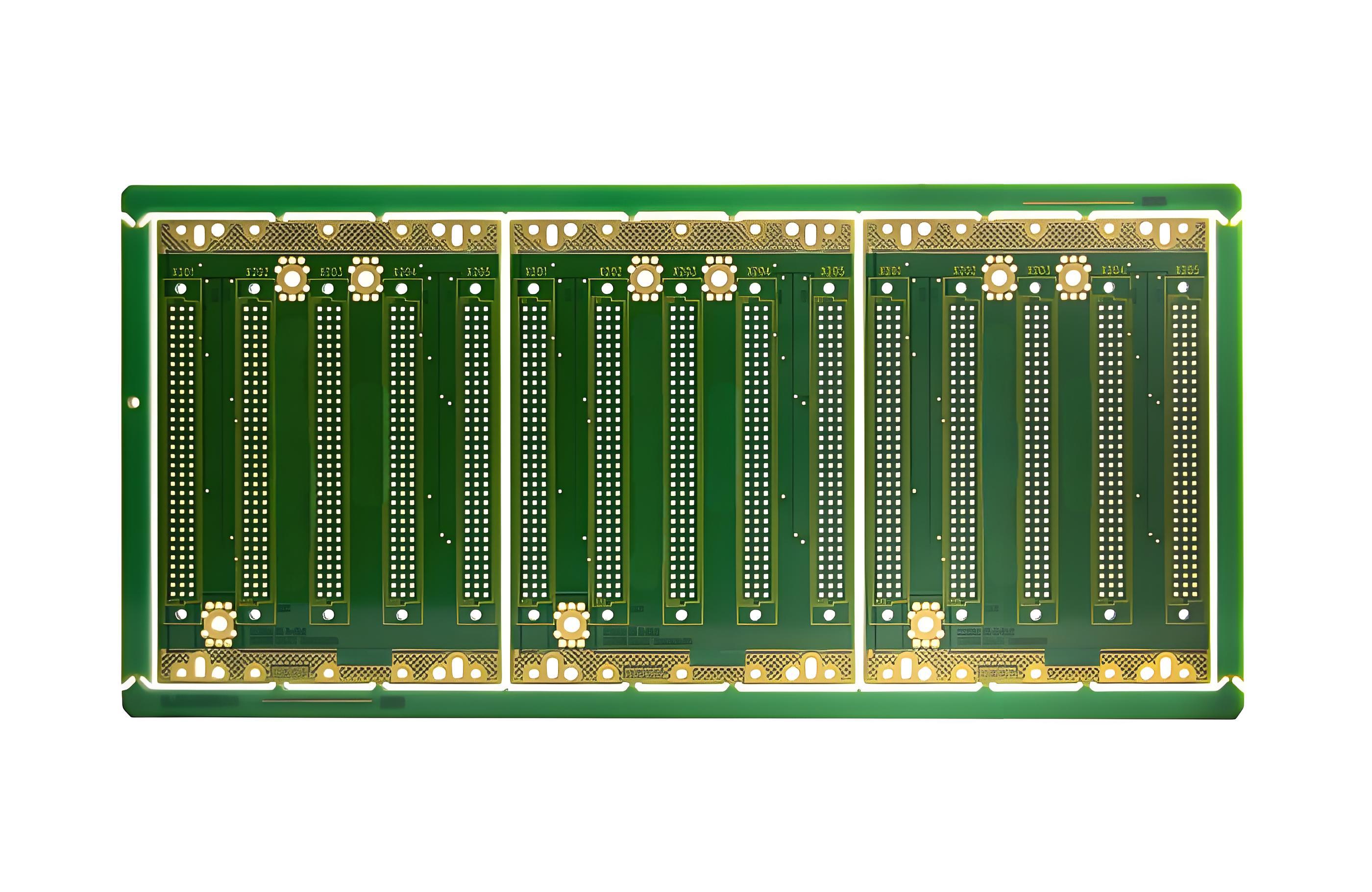
What is a copper coating PCB?
Copper coating in PCB manufacturing creates a conductive pathway by electrochemically storing copper to the surface of the substrate. This process uses a solution of acid-copper sulfate where direct current reduces copper ions to metal shape, the building layer is usually 0.5-3 miles thick for reliable current conduction.
Modern techniques use reversed currents to achieve uniform deposition, especially in the VIAS ratio high aspects, prevent defects while maintaining consistent thickness. The scratching of the scratch containing organic additives that improve the structure of copper seeds to 0.2-0.8îiefm, increase conductivity and mechanical resistance. Process parameters such as current density (15-35 ASF), temperature (20-28 ° C), and copper concentration (40-60 g/L) are strictly controlled to meet industrial standards for signal integrity and thermal reliability.
The advantage of a copper coating pcb
- Increased conductivity: The purity of copper exceeds 99.9%, reduces impedance by 15% compared to copper foil rolled for high frequency signals (> 10 GHz).
- Structural Coverage Ability: Credit coating reaches a uniform coating ‰ ¥ 1î¼m in the holes, eliminating the canceled disability of copper.
- Cost efficiency: Allows the conductive layer of ultra-thin 3-5îiefm, cutting the cost of raw materials by 20% versus lamination of foil.
- Thermal Management: PEEL power> 1.5 N/mm with a CTE match increased by 30% minimizes delamination at high temperatures.
- Design flexibility: Supports the 50î¼m fine line circuit, increasing stomach density by 40% compared to traditional ETSA.
- Environmental Compliance: Cyanide -free process meets Rohs 3.0 standards, reducing wastewater treatment costs by 35%.
- Improvement Ability: The release of the ability to re -cut repair costs up to 1/5 of the cost of replacing foil.
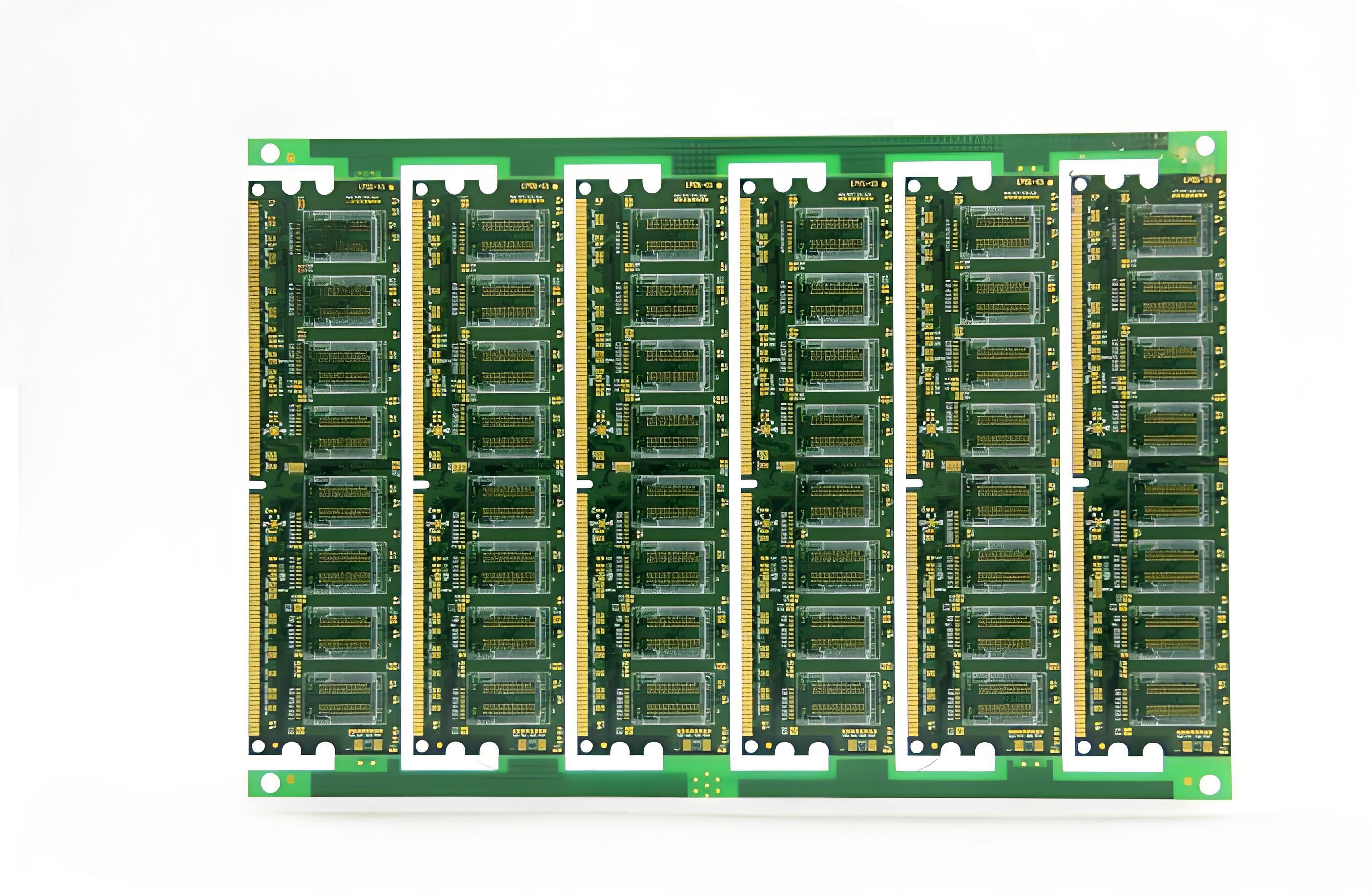
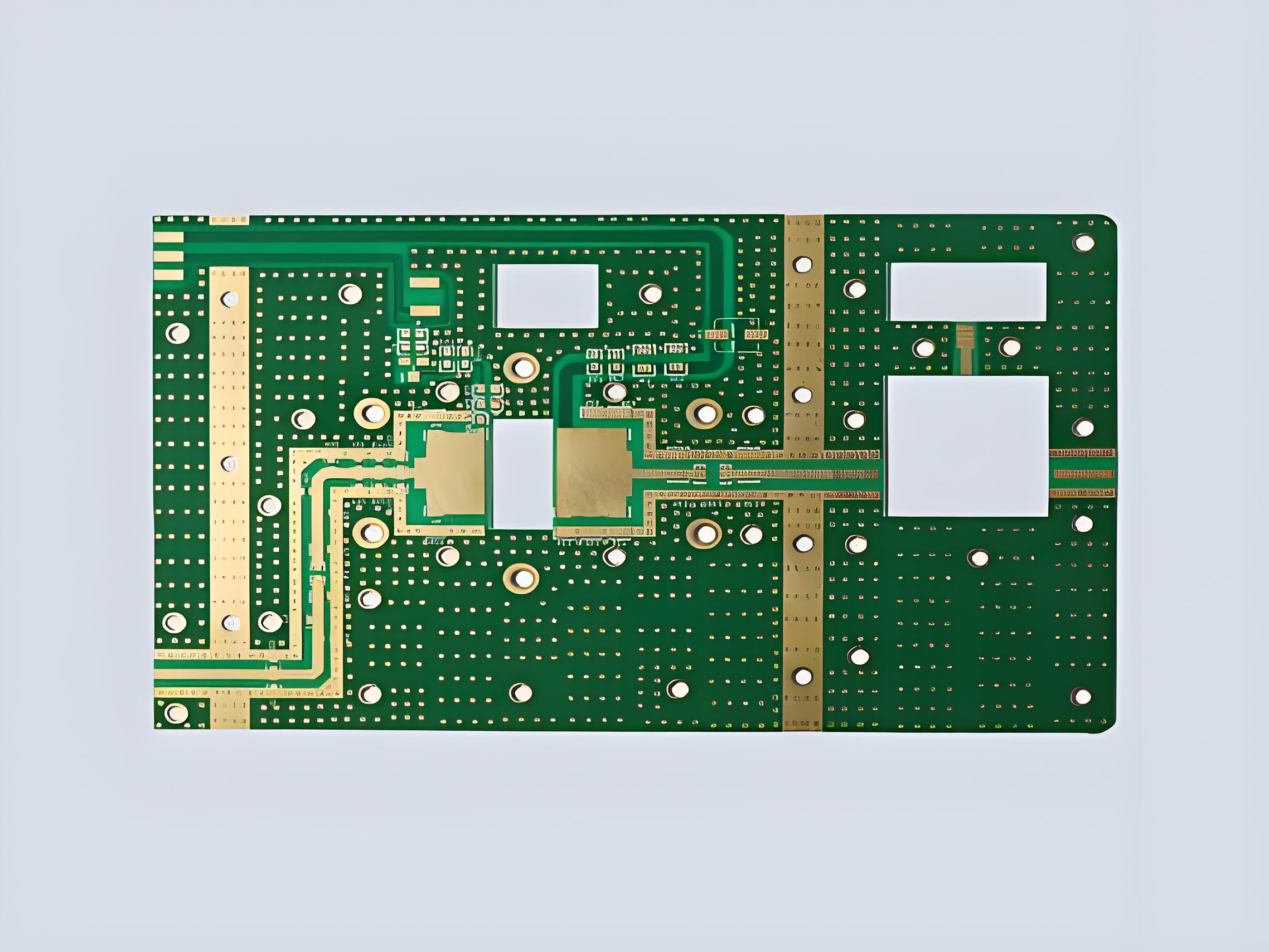
Copper Coating PCB Board Application
- High frequency circuit -Cactive stable signal transmission up to 40GHz for 5G/WiFi-6E application due to ultra-Halus surface layers (RA <0.3îief).
- Electronic power -Supporting the current density 20A/mm² in the Automotive PCB/Industry through adjusted thickness (30-300îîîlen).
- Miniature device -Allows micro-VIA filling 0.1mm for implants that can be subject to/medically using electroplating bottom-up technology.
- Thermal-critical system -Providing 3D heat dissipation paths in the LED/CPU substrate with a filling level of 95%.
- Flexible electronics – Maintaining conductivity after 100,000 bending cycles (R = 3mm) for a folded display.
- High reliability products- Eliminating the failure of the CAF (conductive anodic filament) in the aerospace/military PCB through free coating canceled.
- Applications that are sensitive to costs -Reducing the use of gold by 70% in the peripheral connector through the buildup of selective copper-eMas-eMas.
- High density interconnection – Activating 15îiefm path/space in the chip packaging substrate with the process of coating additives.
- Hard environmental use – Hold 1000 hours of salt spray testing for marine/outdoor applications.
- RF Shielding – Make a smooth EMI cage around the component through a conformed cavity coating.
PCB copper coating method
Below is a method of PCB copper coating:
- Pulse coating – Allows the ratio of aspects of 10: 1 through filling with a uniformity of ± 1îiefm thickness, reducing blind through the risk of canceled by 50%.
- Direct metallization – Eliminating electrical copper steps, processing processing time 40% and wastewater treatment costs 60%.
- Horizontal coating -Ultra-Thin 18îiefm substrate process with a thickness of ± 0.3îiefm, compatible with roll-to-roll production.
- Selective coating -The achievement of the thickness of 100î¼m localized, reducing the use of 70% gold for high clothing connectors.
- Through coating charging -Ansative 100% free charging is canceled, improve thermal cycling performance 3x (Mil-STD-202G).
- Electric copper – Includes 3D irregular structures at the deposition rate of 8îief/hour, adhesion> 1.2kn/m.
- Pattern coating – Form 15îiefm smooth traces with <5îlen undercut, increasing the density of stomach 30%.
- Coating through the hole -Maintain â ‰ ¥ 25îiefm in copper thickness in the ratio hole aspects 10: 1 (IPC-6012 Class 3 appropriate).
- Masked coating – Control regional thickness variations in ± 5%, reducing Etchant consumption 35%.
- High -speed coating – Operates at the deposition level of 10î¼m/minute, increasing productivity 5x for mass production.
PCB copper coating process
1. Surface Preparation ‘
- Microetchingâ € œ:: Creating roughness 1-3îiefm for optimal adhesion (skin strength 180 °> 8n/cm)
- Degreasingâ € œ:: Remove organic contaminants with residues <0.1mg/cm
2. Catalyst application ‘
- Paladium activation ‘:: Deposit 0.02-0.05îiefm the catalytic layer for uniform initiation
3. Deposition of Electric Copper ‘
- Autocatalitic Process’:: Build a layer of seeds 0.3-1 Us at 15-25 ° C (deposition rate 4-6îief/hour)
4. Electrolytic coating ‘
- Dc ‘coating:: Standard 20-40 Us buildup (current density 2-3asd)
- Credit coating ‘:: For HDI boards (aspects ratio> 8: 1, Deviation of thickness ± 5%)
5. Through filling technology ‘
- Reverse pulse ‘:: Achieve free charging canceled in Microvias ‰ ¤100îîief (time of contents <60 minutes)
6. Post -treatmentâ € œThe
- Anti-Tarish ‘:: Organic layer prevents oxidation (salt spray resistance> 96 hours)
- Annealingâ € œ:: Heat treatment 180 ° C increases ductility (extension> 15%)
7. Quality Control ‘
- Cross section analysis’: Measuring the uniformity of the thickness (IPC-6012 Class 3 according to)
- Pull Testing ‘:: Verify> 1kn through barrel power
8. Waste management ‘
- Closed loop systemâ € œ:: Recovery> 95% copper from the drag-out solution
- Each step includes parameters that can be measured directly affect the results, reliability, and cost efficiency.
Why choose the best technology as a PCB manufacturer of copper coating?
The reason why choosing the best technology as Copper coating pcb manufacturer:
- Various surfaces are complete: Mixed finishing support (such as Enig+OSP on one board) to reduce costs by 15-40%
- Fast Prototype 24 Hours: Shorten the R&D cycle by 50% and accelerate the launch of the product
- 1 piece of MOQ: Zero inventory risk, trial production costs are reduced by 90%
- Competitive & transparent prices There is no hidden cost, offering the best value without reducing quality.
- Turnkey Solution â € “Complete PCB Manufacturing Services from Design to Shipping, Speed up the time-to-market of your product.
- ISO 14001/ISO 13485 Certification: Medical/automotive customers are exempt from secondary testing, and compliance costs are reduced by 30%
- DFM Analysis (Design for Production) Free: Optimizing the PCB layout to reduce material waste, lower production costs, and avoid the final design revision.
Types of Our Surface Care Available
Hot Air Solder Leveling (Hasl) “”
- Type ‘:: Lead (environmentally friendly), contains lead (traditional).
- Features’:: Low cost, excellent solder capability, suitable for PCB with broad component distances.
- “” Poor surface circles, not suitable for fine pitch components with high density.
Preservatives of Organic Sutderability (OSP) “
- Principleâ € œ:: Forming organic protective films on copper surfaces to prevent oxidation; environmentally friendly.
- Profit “: Simple processes, low costs, high surfaces.
- Applicationâ € œ:: High frequency signal transmission and lead -free polishing scenario.
Electric Nickel Soaking Gold (ENIG) “
- Structure ‘:: Nickel layer (3-6îief) + gold layer (0.05-0.15îief).
- Profit “: Very good delights, strong corrosion resistance, ideal for high -class products (for example, BGAS, smartphone motherboard).
- Riskâ € œ:: Potential phenomenon “black” pad (nickel corrosion) which requires process control.
Silver immersionâ € œThe
- Characteristics’:: Surface roughness <0.12îief, suitable for high frequency signals (5g/mmwave).
- Profit “: Excellent conductivity, fast processing, cost -effective.
- Noteâ € œ:: Requires prevention of sulfurization and storage environment control.
Immersion Tinâ € œThe
- Profit “: Extensive solder compatibility, lead free, flat surface.
- “” Short storage life (usually ‰ ‰ ¤6 months), tin mustache control needed.
Hard gold coating “
- Applicationâ € œ:: High clothing scenarios (for example, gold radius, connector).
- Propertyâ € œ:: Gold thickness â ‰ ¥ 0.3îief, hold> 10,000 insertion cycles.
- Processâ € œ:: Requires nickel underplating to prevent diffusion.
Electric Electric Nickel Electric Paladium Soaking Electric (Enepig) â € œ
- Structure ‘:: Nickel + palladium + gold triple layer, removing the black enig pad defect.
- Profit “: Strong thermal stability, suitable for some reflows and chip packaging.
How do you get an offer for your PCB project?
PCB Specifications Requirements
1. Details of basic ingredients
- Types of boards (FR-4, high frequency, flexible, etc.)
- Thickness requirements (standard 1.6mm or specific)
- Copper weight (for example, 1oz, 2oz)
2. Design parameters
- Quantity requirements (prototype/bulk)
- Board dimensions (max/min size)
- Number of layers (single/double/multi-layer)
- Minimum trail/space width
- Hole specifications (layered/not layered, size)
3. Selection of Surface Care (Available Option References)
- The Final Type you like
- Special Requirements (eg Enig with> 5 Us Nickel)
- Treatment of Peripheral Connectors if it applies
4. Special process
- Impedance control requirements
- Through treatment (tents, installed, etc.)
- Silk color/legend
- Color and Type of Solder Mask
5. Testing & Certification
- Electric testing requirements (Flying Probe, AOI)
- IPC class requirements
- Special Certification (UL, Rohs, etc.)
6. Delivery requirements
- Target delivery date
- Packaging specifications
- Delivery destination
7. Additional documentation (attach if available)
- Gerber File (RS-274X is preferred)
- Bore file
- Stack diagram
- Special instruction document
Welcome to contact the best technology to get free offers for your PCB project: [email protected].
Tags: copper coating pcb, copper coating pcb board
This entry was posted on æÿœœäºœ, 22 7 æœ Monday, 2025 at 9:14 丸Šˆ and submitted under the best PCB, BestTPCB, PCB Technology. You can follow any response to this entry through RSS 2.0 bait. You can leave a response, or trackback from your own site.
Game Center
Game News
Review Film
Berita Olahraga
Lowongan Kerja
Berita Terkini
Berita Terbaru
Berita Teknologi
Seputar Teknologi
Berita Politik
Resep Masakan
Pendidikan
Berita Terkini
Berita Terkini
Berita Terkini
review anime
Gaming Center
Originally posted 2025-07-22 04:39:55.