Look for Extreme copper PCB Solution? This guide includes specifications, benefits, applications, and design guidelines for extreme copper PCB.
Are you having a problem with this problem?
- PCB failures are often in high -current scenarios?
- What is the cost of cooling solutions out of control?
- Half age in a hard environment?
The best technology can provide solutions:
- 4-20oz Copper layer Step: The minimum trail width of 0.8mm reaches 600a continuous current.
- 3D Heat Dissipation Topology: 0.5mm microvia cluster + copper pillar solder, reduce thermal resistance by 40%.
- A layer that can be adjusted to the environment: Passing multiple tests 85 72 hours, IP67 protection rate.
Welcome to contact us if you have a request for a heavy copper PCB: [email protected].
What is an extreme copper PCB?
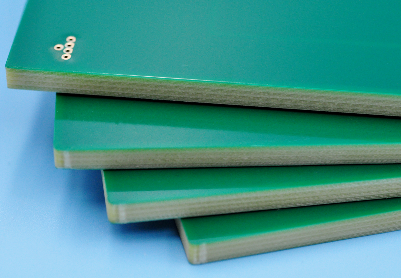
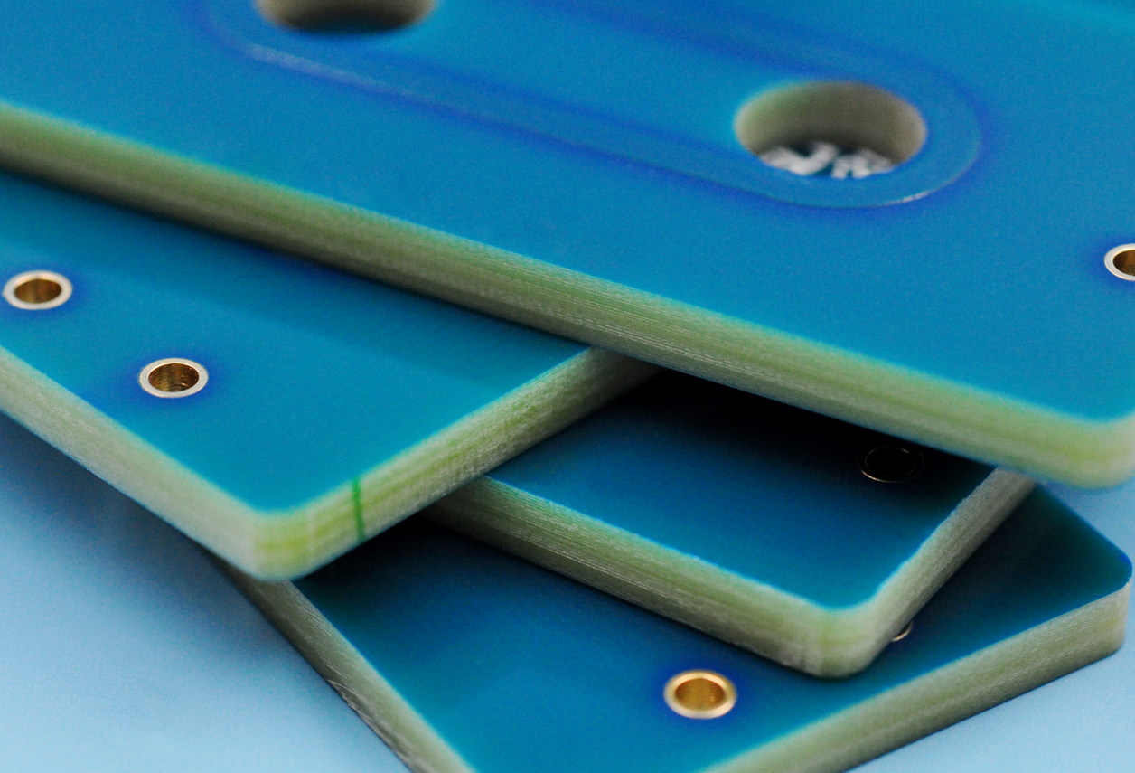
A Extreme copper PCB is a special type of printed circuit board that uses extra thick copper layers, usually starting from 5 ounces/ft ² (around 175 microns) and rises to 20 ounces/ft ² or even higher. This thick copper layer is far larger than the standard 1 or 2 oz copper found in most PCBs. The purpose of using extreme copper is to handle very high currents, manage intense heat, and ensure mechanical endurance in a hard environment.
Unlike standard copper PCB boards, extreme copper PCBs can safely carry out large currents without overheating, thanks to an increase in the cross -sectional area of copper traces. In addition, thick copper increases thermal conductivity and mechanical strength of the board, making it very reliable for long -term use in demanding applications.
Extreme copper pcb specifications
| Parameter | Specification |
| Copper thickness | 5 ounces/ft ² to 20 ounces/ft ² (175 μm to 700 μm) |
| Basic material | TG TG is high, polyimide, metal nucleus (aluminum or copper), ceramics |
| The thickness of the board | 1.6 mm to 6.0 mm (adjusted) |
| Minimum width/distance | 0.5 mm / 0.5 mm (can vary based on thickness and copper design) |
| Maximum current capacity | Up to 100 amp or more, depending on the width of the trail and weight of copper |
| Thermal conductivity | Height, due to thick copper and thermal VIAS (1,0â € “3.0 W/Mâ · K for FR4 standard) |
| Surface final option | Enig (Gold Immersion), Hasl, OSP, Silver, Hard Gold |
| Drill hole size | Minimum 0.3 mm (12 million), larger holes are recommended for thick boards |
| Number of layers | 1 to 6 layers (usually 1 € “2 layers for extreme copper) |
| Impedance control | Maybe with a careful design; maybe challenging because of thick copper |
| Solder mask | Hold high temperatures (for example, green, black, white, special color) |
| Type of coating | Heavy copper coating for traces, pads, and holes through |
| Thermal through support | Yes – often needed for heat dissipation in multilayer or dense design |
| Standard compliance | IPC-6012 Class 2/3, Rohs, Ul94-V0 Flame Retardant Rating |
What are the benefits of extreme copper PCB?
Violation
- A single copper layer 4oz (140îief) can carry 50A, four times the current PCB 1Oz PCB.
- Multi-layer buildup solutions (such as a combination of 2oz + 4oz) support high-current transmission that exceeds 1000A.
Reducing the risk of rising system temperature
- The test shows that under the same load, the increase in the temperature of the 4oz copper plate is 40% lower than the 1 oz copper plate.
- Reducing the size of the Heat Sink allows miniaturization of devices.
The extended product life cycle
- The strength of the fatigue of the copper layer increases 60%, preventing the cracks of the circuit caused by high frequency vibrations.
- Salt spray tests show corrosion resistance is three times the conventional PCB.
The complexity of simplified system design
- Some low -voltage circuit boards can be combined into a single board, reducing cable connectors and harness.
- Supports integrated power/signal design, reducing EMI disorders.
The advantage of the cost of the life cycle
- Although the initial cost increased by 20%, the failure rate decreased by 70%.
- TCO calculation (total total ownership cost) five years shows a reduction of 35% in maintenance costs.
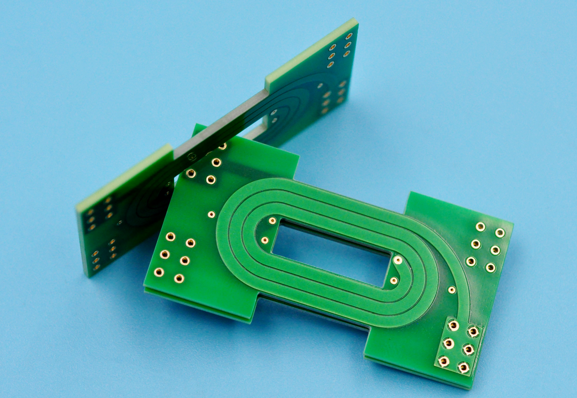
What is the extreme copper PCB application?
Extreme copper pcb application
- Electronic power“Used in power supply, converter, and inverter to handle high currents and heat.
- Automotive systemIdeal for electric vehicle charging, battery management system, and motor controller.
- Industrial equipment“Applied to welding machines, heavy machines, and high power control systems.
- Military and aerospaceâ € “used in radar systems, communication devices, and rough electronics for hard conditions.
- Renewable energyâ € “found in solar inverters and wind power controls that require high reliability and heat resistance.
- Trains and transportation“Used in power control units and signaling systems that require a strong and durable PCB.
- Medical devicesSuitable for high -power medical equipment that requires stable and safe operations.
Extreme heavy copper pcb design guide
1. Selection of material
- Basic material: Use high TG (‰ ¥ 180 ° C) FR4 or PTFE filled with ceramics for thermal stability.
- Copper foil: Determine 6-10 oz (210-350 µm) Anil copper is rolled up for flexibility and adhesion.
- Metal core: Integration of aluminum/copper substrate (eg 2mm thickness) for direct heat dissipation.
2. Stackup Strategy Layer
- Outer layer: 6-10 oz copper for power/land.
- Inner layer: 2-4 oz copper for signals; Add isolated power aircraft for high current rails.
- VIAS Thermal: Place Vias with a diameter of 0.8-1.2mm (‰ ¥ 3 oz plating) under the heat component to connect the outer/inner layer.
3. Rules of Traces Design
- Calculate the width using IPC-2221 (for example, 10 oz copper = ~ 150a for a trace of 20mm at an increase of 10 ° C).
- Use 45 ° bends; Avoid the right corner to reduce the surge in impedance.
- Thickening traces near the connector (for example, nominal width 2x) to handle surge.
4. Thermal management
- The contents of the area that is not used by pouring copper (¥ 70% coverage) is bound to a ground/power aircraft.
- Use the embedded heat sink (for example, copper coins) under the mosfet/IGBT.
- For metal-core boards, bonding components directly to the substrate with thermal epoxy.
5. Power distribution
- Split Power Planes based on voltage (for example, 48V, 12V) to minimize noise.
- Place decoupling capacitors (for example, ceramics 10 μF) in 2mm from IC power pin.
- Spread the battery-to-be-free pathway (for example, a trace of 50mm+) to minimize the decrease in IR.
6. Signal integrity
- Keep a high -speed trail (> 100MHz) from the power zone (‰ ¥ 5mm gap).
- Adjust the trail distance to maintain the impedance 75-100î © despite the thick copper.
- Use the guards (copper ground) around the sensitive signal.
7. Manufacturing Compliance
- Determine “Extreme Heavy Copper” and “Metal-core” in the design record.
- Confirm the minimum trail/space (¥ 10mil) and through the size of the drill (‰ ¥ 0.5mm).
- Ask differential ETSA and X-Ray inspection to go through the quality of the coating.
8. Assembly considerations
- Use high temperature solder (for example, SAC305) is assessed for 260 ° C reflow.
- Add the solddermask dam between thick traces to prevent solder wicking.
- Test prototype with a 2x nominal current to validate thermal performance.
9. Validation & Testing
- Perform thermal imaging under the max load to identify the overheating zone.
- Use microsection analysis to verify the thickness of copper and through coating integrity.
- Perform termination (highly accelerated life test) for thermal cycling (-40 ° C to +125 ° C).
Why choose the best technology as an extreme copper PCB supplier?
The reason why choosing us as Extreme copper PCB supplier:
- Certified Compliance (ISO 9001, UL, Rohs) – Reducing regulatory risk and ensuring products meet global standards for environmental safety and compliance.
- 19 years of heavy copper PCB manufacturing experience – Fast and flexible handling thick copper plate production, accelerating the production cycle
- 24 -hour fast prototype delivery -The acceleration of the product development cycle, allows faster time to the market and competitive advantage in the high demand industry.
- Strict quality control with 100% inspection -Eliminating hidden defects, reducing re -work costs, and ensuring reliability in high/thermal application.
- Transparent price without hidden costs – Predicted budgeting and cost savings through the face setting model that is adjusted to the specifications of the thick copper PCB.
- DFM Analysis (Design for Production) Free -Pimin the PCB layout to reduce material waste, lower production costs, and avoid the final design revision.
- One -roof solution from design to shipping – streamline project management by consolidating prototyping, fabrication, and assembly under one roof.
Our heavy copper PCB capabilities
| Basic material | FR4/Aluminum |
| Copper thickness: | 4 oz ~ 10 ounces |
| Extreme heavy copper: | 20 ~ 200 ounces |
| Outline: | Routing, punching, V-Cut |
| Solddermask: | White/black/blue/green/red/red oil |
| Surface finishing: | Gold Immersion, Hasl, OSP |
| Max panel size: | 580*480mm (22.8 ″*18.9 ″) |
How do you get an offer for extreme copper PCB projects?
Basic structural parameters
- The number of layers required (one side/two sides/4-20 layers)
- The dimensions of the finished product (length x width ± tolerance) and panelization plan
- Panel Type (FR4 Tg 170â °/Aluminum Substrate/Ceramic Substrate
- The thickness of the target board (range 0.8-6.0mm)
Copper foil process specifications
- Distribution of copper thickness (for example, outer layer 4oz/2oz inner layer)
- SPECIAL REQUIREMENTS (Copper Blocks Local/embedded Copper Value)
- Minimum width/distance (for example, 6oz copper thickness requires ‰ ¥ 5.0mil)
Electric Performance Requirements
- Current power capacity (for example, continuous current ‰ ¥ 200a @ 25 ° C)
- Impedance Control Requirements (Differential and Tolerance Pair Impedance Value)
- Insulation holds voltage ratings (Voltage DC/DC Frequency)
Surface final option
- Select one: Enig/Tin Immersion/OSP
- Solder Mask Color (Default Green, Other Colors +20%Cost)
- SILKSCREEN REQUIREMENTS (Character High â ‰ ¥ 0.8mm)
Special process instructions
- Thick copper etching compensation solution (required design documents)
- Thermal via design (diameter/pitch/aperture filler)
- Reception Criteria (IPC-6012D) Class 2/3)
Required documents
- Gerber (RS-274X format) + Bore File.
- Stackup Diagram (with copper thickness distribution).
- Impedance calculation table (if a high -speed signal is involved).
Why choose the best technology?
- 19 years of thick copper expertise: Give more than 50 million 4oz+ PCB since 2006, strategic suppliers to Tesla and Huawei.
- Price transparency: The supply chain that is integrated vertically, the price of 30-40% is lower than European and American producers for comparable processes.
- Extreme Response: Emergency choice 24 hours, shipping first part 72 hours (average industry: 7 days).
- Full Inspection Commitment: 100% AOI + Flying Probe Testing, CPK ‰ ¥ 1,67, Failure Rate <50 ppm.
- One -stop service: From design reviews to conformal layers to assembly and testing, complete management.
Welcome to contact us if you have a Copper PCB request: [email protected].
Tag: extreme copper PCB, extreme copper PCB supplier
This entry was posted on Tuesday, July 29, 2025 at 18:31 and submitted under the best PCB, BestTPCB, PCB Technology, Special PCB. You can follow any response to this entry through RSS 2.0 bait. You can leave a response, or trackback from your own site.
Game Center
Game News
Review Film
Berita Olahraga
Lowongan Kerja
Berita Terkini
Berita Terbaru
Berita Teknologi
Seputar Teknologi
Berita Politik
Resep Masakan
Pendidikan
Berita Terkini
Berita Terkini
Berita Terkini
review anime