How do I design one -sided copper PCB? Let’s find specifications, benefits, design guides, and manufacturing process for one -sided copper PCB board.
Are you having a problem with this problem?
- Is insufficient heat dissipation leading to shorter product age?
- Is the loss of high frequency signal transmission that affects performance?
- Is it difficult to balance the reduction and reliability of costs?
The best technology can provide services and solutions:
- Using aluminum-conductivity substrates high-conductivity (thermal conductivity ‰ ¥ 2,0 w/mâ · k) and optimizing the thickness of copper foil, we have reached a measured temperature reduction 15-30 ° C.
- The constant dielectric substrate is low-K and proper impedance control (± 5%tolerance) ensures stability in high frequency scenarios such as 5G and radar.
- The smart layout algorithm and the standard material library reduces the cost of mass production by 20% and passed the 5,000 hour Burn-in test.
Welcome to contact us if you have a request for PCB Core Metal: [email protected].
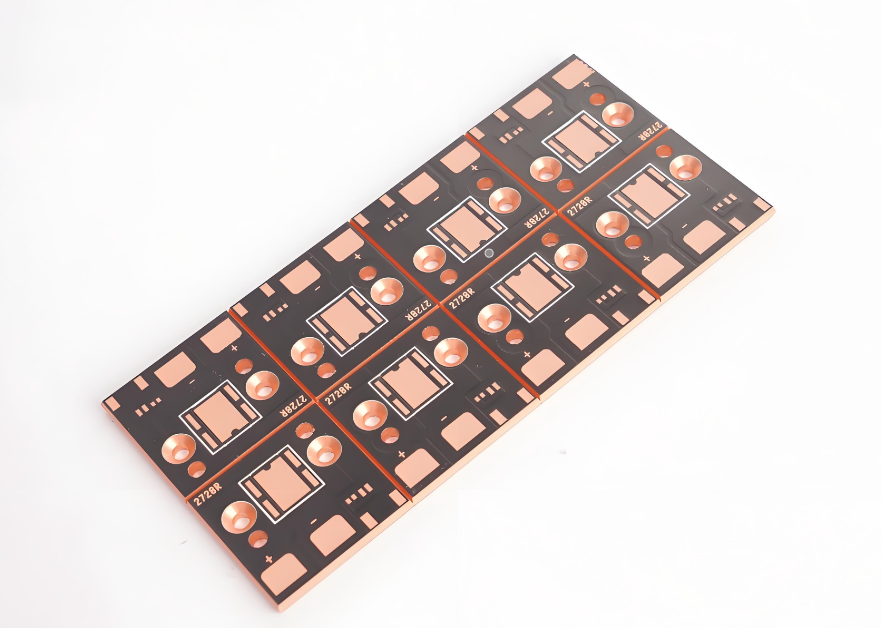
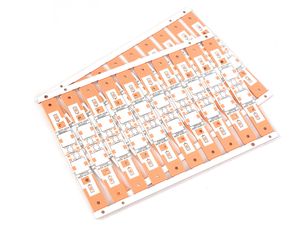
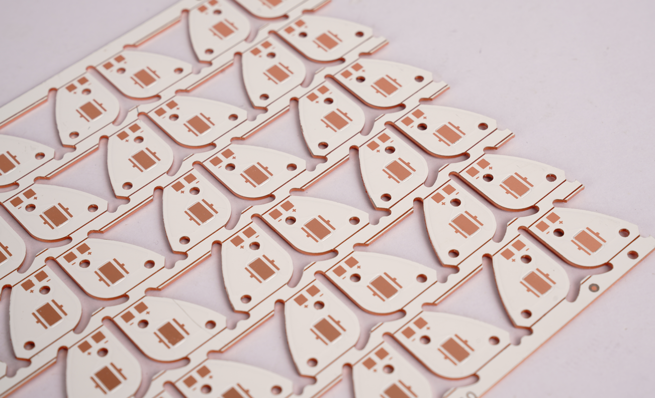
What is one -sided copper PCB?
A “PCB Copper Single Side ‘ Is the simplest type of circuit board printed, which consists of a single conductive copper layer that is bound to one side of the isolation substrate (usually F-4 fiberglass or phenolic material). The opposite side remains not coated, making it ideal for direct circuits. The component is installed and soldered to the copper side, while the trail (circuit path) is made by getting an unwanted copper.
Single copper pcb specifications
| Parameter | Specification |
| Basic material | FR-4 (Retardant 4) or phenolic paper |
| Copper thickness | 18 î¼m (0.5 oz/ft ²) up to 35 î¼m (1 ounce/ft ²) |
| Track width/distance | Minimum 0.2 mm (8 million) for traces; 0.15 mm (6 million) for distance |
| Solder mask | Liquid Photoimageable (LPI) or Mask Solder Film Dry (Optional) |
| Silkscreen | White, black or yellow (optional) ink |
| Final surface | HASL (Hot Air Soldering Leveling), Enig (Electric Nickel Soaking Gold), or OSP |
| The thickness of the board | 0.8 mm to 1.6 mm (standard) |
| Thermal resistance | TG 130 ° C (FR-4 Standard) |
| Impedance control | Not valid (single layer design) |
| Peel strength | ‰ ¥ 1.0 kgf/cm (copper-to-substrate adhesion) |
| Flammable ranking | UL-94 V-0 (Self Self) |
| Applicable standards | IPC-6012 (Class 2/3), Rohs, Reach |
The advantage of one -sided copper PCB
- Low cost -Simplified materials and processes reduce costs by 30% -50% compared to two -sided PCBs, making it suitable for budget -conscious projects.
- Easy design entry -The one side simplifies the circuit design, allowing even novice designers to quickly design and shorten the prototype verification cycle.
- Fast production -Sle slender process and high level of automation allows shipping 3-5 days for regular orders and 24-hour delivery for urgent orders.
- Low failure rate – There is no VIAS connection or interlayer, producing minimal signal disorders, high temperatures and humidity resistance, and high reliability in the industrial environment.
- Obey the environment -Recycled materials, no electroplating contamination, and Rohs compliance/range ensures free exports are worried.
- Flexible customization – Adjustable substrate, surface maintenance, and color meet the differentiation of certain brands or environmental requirements.
- Broad application -Swear household appliances, consumer electronics, industrial control, and other fields, this solution provides a one -stop solution for the needs of low to medium density circuits.
One side copper pcb board application
- Household appliances – Washing machine, refrigerator, microwave oven (simple control circuit).
- Consumer Electronics – Electronic toys, basic long distance control, LED lighting drivers.
- Industrial control -The low complexity, motor control, power distribution unit.
- Automotive electronics -The lighting system, low -speed electric vehicle battery management.
- Power supply -Low -cost adapters, simple charger circuits (low density design).
- Medical devices -Basic diagnostic tools, portable health monitors (non-critical circuits).
- IoT & Smart Home -Entry-level smart pressure, temperature/humidity monitor (low data design).
How do you design a copper PCB with one side copper?
PCB design dressed in one side copper guide:
1. Catching the scheme
- Use the Eda tool (for example, kicad, eagle) to arrange the circuit.
- Set footprints to the component, prioritize the hole through one -sided compatibility.
2. Placement of components
- Set components to minimize traces crossover.
- Place critical components (for example, connectors, power regulators) near the edge of the board.
- Group -related components (for example, decoupling capacitors near ICS).
3. Routing strategy
- The route trail on the copper layer uses a horizontal/vertical grid to avoid overlapping.
- Use jumper or 0î © resistor for an unavoidable crossover.
- Maintain ‰ ¥ ¥ 0.3mm trail width for the signal, ‰ ¥ 1mm for the electric channel.
- Avoid sharp 90 ° angle; Use 45 ° bends.
4. Party/Power Package
- Make a copper pour for GND, making sure thermal relief for hole bearings.
- Analog/digital isolates if needed.
5. Design Rules Check (DRC)
- Adjust the rules of clearance (for example, 0.2mm trace-to-pad, 1mm trace-to-board edge).
- Run DRC to improve violations (for example, short circuits, insufficient distances).
6. Generation of Gerber Files
- Top copper layer (.gtl)
- Solder mask layer (.gts)
- Silkscreen layer (.gto)
- Outline of the board (.gko)
7. Fabrication preparation
- Print layout in transparency films (scale 1: 1) for UV exposure.
- Cut the board wrapped in copper into size, clean with steel wool.
8. Final Inspection
- Check a broken trail, a hole that is not in harmony, or the remaining copper.
- Test continuity and isolation with a multimeter.
How do I make one -sided copper PCB board?
The production process of a single copper PCB Plad
1. Cutting material
- Cut a large copper panel into a production size board, optimizing the use of material.
2. Drilling
- Machine holes for components and alignment using CNC drill. Laser drilling can be used for high density boards.
3. Image transfer
- Dry film method: Apply photosensitive dry films, explain to UV light through artwork, and develop to form ETCH resistant patterns.
- Screen printing: Directly print anti-Eth-Etch ink, cured to make a protective layer.
4. ETSA
- Delete open copper using Ferric Chloride or AMmonia -based etchant. Precision control of etchant concentration, temperature, and spray pressure is very important to minimize the damper.
5. Strout & Cleaning
- Residual Dry Film/Ink Strip and Rinse Board thoroughly. Dry board to prevent oxidation.
6. Solder & Marking Mask
- Solder holds: Print a green solder mask (or color), UV-cured to protect the area that is not overdone.
- Silkscreen: Print white legend for identification of components and polarity signs.
7. Final surface
- Apply the final touches such as HASL (spray tin), Enig (Nickel Chemical/Gold), or OSP (Organic Solderability Preservatives) to protect the bearings and increase solder capabilities.
8. Profile
- The shape of the board through CNC routing or V score for easy separation.
9. Inspection & Testing
- Electric testing: Fly-probe test or bed for conductivity and isolation.
- Visual inspection: AOI (Automatic Optical Inspection) or manual examination for defects (shorts, open, misalignment).
10. Packaging
- Vacuum seal boards with desiccant and include quality certificates.
Why Choose the Best Technology as a PCB Manufacturer Copied?
Reasons why to choose us as a PCB manufacturer wrapped in copper:
- Certified Compliance (ISO 9001, UL, Rohs, ISO 9001, IATF 16949): Reducing regulatory risk and ensuring products meet global standards for environmental safety and compliance.
- Fast Prototype Service: 24 hour turnover for samples with the same day technical review.
- Competitive price structure: Transparent prices without hidden costsâ € “cost effective for high volume production.
- DFM Analysis (Design for Production) Free: Optimizing the PCB layout to reduce material waste, lower production costs, and avoid the final design revision.
- Turnkey Solution â € “Complete PCB Manufacturing Services from Design to Shipping, Speed up the time-to-market of your product.
- Strict quality control: 100% Automated Optical Inspection (AOI) and X-ray testing for defective PCB.
- Fast production waiting time: The standard waiting time of 15 days with accelerated options for urgent orders.
- Custom Material Solution: Dielectric formulation that is adjusted for certain thermal/electricity needs.
- Dedication Technique Support: 24/7 Technical Team to optimize design and problem solving.
Our copper pcb board capabilities
| Basic material: | Copper |
| Thermal conductivity (dielectric layer): | 0.8, 1.0, 1.5, 2.0, 3.0 W/MK |
| The thickness of the board: | 0.5mm ~ 3.0mm (0.02 ″ ~ 0.12 ″) |
| Copper thickness: | 0.5 oz, 1.0 ounces, 2.0 oz, 3.0 oz, up to 10 oz |
| Outline: | Routing, punching, V-Cut |
| Solddermask: | White/black/blue/green/red/red oil |
| Legend/silkscreen color: | Black and white |
| Surface finishing: | Gold Immersion, Hasl, OSP |
| Max panel size: | 600*500mm (23.62 ″*19.68 ″) |
| Is packing: | Vacuum/plastic bag |
| Sample l/t: | 4 ~ 6 days |
| MP L/T: | 5 ~ 7 days |
How do you get an offer for your Metal Core PCB project?
Important Submission Check List
- Design file: Gerber layer, drill data (excellon), assembly image.
- Specification: Basic material (aluminum/copper), core thickness (0.5â € “3.2mm), copper weight (1â €” 4oz).
- Electricity Needs: Max Current (A/Mm²), Control Impedance (± 5%), through the type.
- Surface finishing: Hasl, England, or OSP.
- Quantity & Time Limit: Prototype (1â € “10 pcs) or mass production (> 100 pcs), standard (15 days) or accelerated (7 days).
Why choose the best technology?
- Free DFM Review: Optimizing designs for costs and manufacturing.
- Instant Price: Quote in one day.
- Certified Quality: Compliance with IPC-A-600, UL, and Rohs.
E-mail [email protected] With your specifications for fast and transparent quotes. Let the expertise of PCB Metal Core Best Technology to turn on your innovation!
Tag: PCB Clad Copper Single Side, PCB Copper Single Side
This entry was posted on Wednesday, July 30, 2025 at 18:30 and was submitted under the best PCB, BestTPCB, MCPCB, PCB Core Metal. You can follow any response to this entry through RSS 2.0 bait. You can leave a response, or trackback from your own site.
Game Center
Game News
Review Film
Berita Olahraga
Lowongan Kerja
Berita Terkini
Berita Terbaru
Berita Teknologi
Seputar Teknologi
Berita Politik
Resep Masakan
Pendidikan
Berita Terkini
Berita Terkini
Berita Terkini
review anime