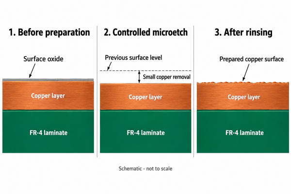
PCB microetching removes a controlled, shallow amount of exposed copper to prepare its surface for a subsequent manufacturing step. It helps remove surface oxidation and establish a suitable copper surface without stripping away the conductor. For a finished board, the important balance is adequate surface preparation without consuming too much of the copper needed for the circuit.
What Is PCB Microetching?
A copper microetch chemically dissolves the outermost copper surface. Micro etching PCB copper can also develop a microscopic texture that helps the next coating or deposited metal attach, depending on the chemistry. The amount removed is small compared with the full copper thickness, but it still belongs in the manufacturing copper budget.
The terms microetching, micro etching and micro etch describe this surface-preparation operation. A microetch PCB process does not mean manufacturing an unusually small board. Its purpose is to prepare exposed copper, whether that copper is on a panel, a pad or an accessible interconnection surface.
How Does Microetching Differ from PCB Etching?
Pattern etching creates the circuit by removing unwanted copper through the foil thickness. Microetching prepares copper that generally needs to remain. Confusing the two can lead to an inappropriate dwell time or an incorrect assumption that a shiny surface proves the circuit dimensions are unchanged.
| Process | Main task | What must remain controlled |
|---|---|---|
| Pattern etching | Remove unprotected copper to form traces and spaces | Conductor width, spacing and undercut |
| Microetching | Remove a shallow surface layer from exposed copper | Copper loss, surface condition and uniformity |
| Cleaning/degreasing | Remove oils and other process contamination | Cleanliness and compatibility with following steps |
| Desmear | Remove drilling-related resin residues | Hole-wall and interconnection cleanliness |
Some proprietary products combine cleaning and microetching. That does not make every microetch bath a substitute for degreasing, and copper microetching alone does not replace resin desmear.
Where Is Microetching Used in PCB Manufacturing?
Microetch treatments can appear before photoresist application, selected plating operations and final surface-finishing steps. The required surface is determined by what comes next: a resist must adhere, a deposited metal must form a sound interface, and a final finish needs properly prepared exposed copper.
These are separate process locations, not instructions to send every board through the same treatment repeatedly. Masked areas, exposed pads and plated features can have different exposure histories. For our FR4 PCB manufacturing, the drawing’s finished copper and conductor requirements are the relevant product targets; the process route must deliver those targets after all copper-removal steps.
Which Chemicals Are Used for Copper Microetching?
Common commercial approaches include stabilized sulfuric-acid/hydrogen-peroxide systems and persulfate-based systems. Proprietary additives influence bath behavior and the resulting surface. Selecting a chemistry therefore involves compatibility with the next process, available equipment and the acceptable copper loss, not just choosing an oxidizer name.
| Chemistry family | Practical consideration |
|---|---|
| Sulfuric acid with stabilized hydrogen peroxide | Oxidizer condition, acid balance and copper loading affect process control |
| Persulfate-based microetch | Concentration, bath loading and treatment conditions influence removal |
| Proprietary surface-preparation formulations | Surface morphology may differ even at a similar removal depth |
An operating temperature or copper-loading limit belongs to a specific product and line setup. Transferring a value between different formulations can change both removal and surface texture. Production chemistry also requires the specified handling, ventilation and waste-treatment controls; an acid-and-oxidizer mixture is not a general workshop cleaning recipe.
How Much Copper Should Microetching Remove?
There is no single removal depth that fits every PCB process. The target must provide sufficient preparation while preserving the minimum required copper and feature dimensions. A thin starting copper layer has less allowance for repeated treatments than a substantially thicker layer.
Three quantities are easy to confuse:
| Quantity | Typical unit | What it describes |
|---|---|---|
| Copper removal depth | Micrometers, written as µm | Average thickness dissolved during a treatment |
| Etch rate | µm/min | Removal per unit time under stated conditions |
| Surface roughness | A defined parameter such as Ra or Rz, in µm | Profile variation, not the amount of copper dissolved |
| Finished copper thickness | µm | Copper remaining after the relevant manufacturing operations |
For example, a measured rate of 1 µm/min over a 30-second exposure predicts 0.5 µm removal only while the rate and exposure conditions remain applicable. This arithmetic is not a recommended process setting. A roughness value of 0.5 µm is not interchangeable with 0.5 µm of copper removal.
How Is the Microetch Rate Measured?
One approach uses the mass loss of a copper coupon with a known exposed area. The coupon is weighed before treatment and again after the prescribed rinsing, drying and conditioning. Residual water, removable contamination or a change in the laminate’s moisture content can distort a small mass difference, so sample preparation must be repeatable.
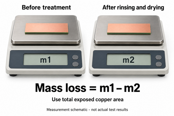
For a measurement in which the lost mass is copper:
Average removal (µm) = 10,000 × copper mass loss (g) / [copper density (g/cm³) × total exposed copper area (cm²)]
Average etch rate (µm/min) = average removal (µm) / exposure time (min)
Using a copper density of 8.96 g/cm³, a hypothetical mass loss of 0.0896 g over 100 cm² of exposed copper gives 1 µm average removal. If treatment lasted one minute, the average rate is 1 µm/min. These are calculation inputs, not our factory test results.
Count all exposed copper surfaces. If two faces are each 50 cm², their combined area is 100 cm², before considering any other exposed copper. Using only one face would double the calculated depth incorrectly. Coupon copper type, pretreatment and exposure must also be representative: foil and plated copper need not dissolve at identical rates.
The result is an average. It cannot prove how much copper was removed at one narrow trace edge or at the bottom of a blind microvia.
What Changes the Microetch Rate?
Temperature and dwell time are only part of the answer. Bath composition, dissolved copper, solution movement and the condition of the incoming copper can change the result. A conveyor speed establishes nominal exposure, but it does not establish that every nozzle is delivering the same flow.
When removal changes unexpectedly, a useful troubleshooting sequence is:
- Confirm the coupon area, timing, weighing and drying procedure before adjusting the bath.
- Compare actual bath temperature and chemistry analysis with the approved operating range.
- Check loading, replenishment history and the incoming surface condition.
- Inspect spray coverage or immersion circulation, including panel placement.
- Repeat the measurement under the corrected conditions and compare different positions where necessary.
Changing several variables together makes the cause difficult to identify. Increasing dwell time may compensate for a weak average rate while leaving a poor-flow location inadequately treated.
What Happens If Copper Is Overetched or Underetched?
Insufficient preparation can leave an unsuitable interface for the next operation. Excess removal can reduce the available copper thickness or alter exposed conductor geometry. Neither condition should be diagnosed from copper color alone.
| Observation | Checks that help narrow the cause |
|---|---|
| Poor resist or coating adhesion | Incoming cleanliness, preparation, application and cure conditions |
| Uneven copper appearance | Wetting, flow distribution, contamination and panel exposure |
| Excess coupon mass loss | Timing, area calculation, temperature and bath analysis |
| Narrow traces or thin copper after processing | Accumulated removal across the route, not only the last bath |
| A plating-interface concern | Surface preparation together with activation and plating conditions |
These observations are not one-to-one proof of a microetch fault. For example, adhesion can fail because of contamination introduced after preparation. Adding another microetch cycle without identifying the cause also adds copper loss and may not correct the defect.
How Does Microetching Affect HDI and Fine-Line PCBs?
Fine conductors and thin copper leave less room for unplanned removal. Our HDI PCB manufacturing supports fine-line designs, with line/space capability down to 2/2 mil on suitable constructions. The final stack-up, copper thickness and feature combination still require engineering review; that capability is not a universal microetch allowance.
Microvia geometry creates a further issue: a flat coupon is easier for chemistry to reach than a recessed target pad. Solution exchange and local preparation must be evaluated for the actual feature, rather than inferred solely from a panel-surface measurement.
For impedance-controlled PCBs, finished conductor geometry affects impedance, while copper roughness can also contribute to conductor loss at high frequency. “Rougher is better” is therefore not a complete design rule. Surface preparation must suit adhesion needs without ignoring the specified copper profile and electrical design.
Why Do Rinsing and Transfer Time Matter?
Carryover can contaminate the next bath, and exposed prepared copper can change during an uncontrolled wait. Rinsing, drainage and transfer conditions are part of the process route, not housekeeping after the important work is finished.
Whether a board proceeds wet-to-wet or is dried depends on the next operation. A coupon dried for weighing is not evidence that production boards should always be dried at that point. Likewise, a delay suitable for one finish or resist process cannot automatically be used for another.
How Can Microetching Quality Be Checked?
A useful check links the bath result to the board: verify removal, inspect surface uniformity, and confirm the relevant downstream result. Adhesion, finished dimensions or plating-interface examination answer different questions and should not be replaced by a single average mass-loss number.
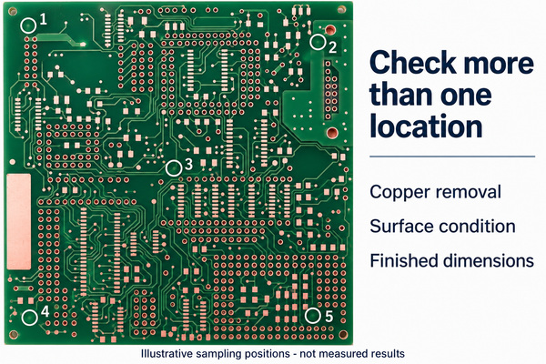
The comparison needs traceable conditions: coupon type and exposed area, exposure time, bath condition, measurement method and panel position. If a thin-copper product is under review, compare its remaining copper with the drawing requirement. If an adhesion issue is under review, examine the relevant coating or interface rather than concluding that a passing thickness measurement resolves it.
At EBest Circuit (Best Technology), we manufacture custom PCBs to the agreed board requirements. Send your stack-up, finished copper thickness, minimum line/space and surface-finish requirements to [email protected] for a manufacturing review. Include any special copper-profile or interface requirements so that pcb microetching and the surrounding process steps are considered against the actual circuit, rather than an isolated bath setting.
PCB Microetching FAQs
How to Do Microetching on a PCB?
Use the qualified preparation sequence for the selected chemistry and next manufacturing step: prepare the incoming surface, apply controlled exposure, rinse as specified and transfer under the defined conditions. A production procedure must specify its operating limits and checks; the mass-loss example above is not a bath recipe.
Can mechanical brushing replace microetching?
Not automatically. Brushing acts mechanically on accessible surfaces; a chemical process acts on wetted copper. Substitution requires confirming surface condition, dimensions and compatibility with the next operation, particularly where a brush cannot reach.
Is microetching the same as black oxide treatment?
No. Both can be associated with copper surface preparation, but black oxide treatment produces a conversion layer for bonding purposes. Microetching removes copper. An oxide-alternative process may include controlled etching, yet its full chemistry and qualification cannot be reduced to the word microetch.
Does a microetch result prove that the finished PCB is acceptable?
No. A pcb microetching result describes one part of fabrication. Finished-board acceptance still depends on the specified dimensions, electrical testing, finish and other applicable product requirements.
Tags: Copper Surface Preparation, pcb manufacturing, PCB Microetching
PakarPBN
A Private Blog Network (PBN) is a collection of websites that are controlled by a single individual or organization and used primarily to build backlinks to a “money site” in order to influence its ranking in search engines such as Google. The core idea behind a PBN is based on the importance of backlinks in Google’s ranking algorithm. Since Google views backlinks as signals of authority and trust, some website owners attempt to artificially create these signals through a controlled network of sites.
In a typical PBN setup, the owner acquires expired or aged domains that already have existing authority, backlinks, and history. These domains are rebuilt with new content and hosted separately, often using different IP addresses, hosting providers, themes, and ownership details to make them appear unrelated. Within the content published on these sites, links are strategically placed that point to the main website the owner wants to rank higher. By doing this, the owner attempts to pass link equity (also known as “link juice”) from the PBN sites to the target website.
The purpose of a PBN is to give the impression that the target website is naturally earning links from multiple independent sources. If done effectively, this can temporarily improve keyword rankings, increase organic visibility, and drive more traffic from search results.
