When you see a printed circuit board (PCB), you might see a shiny metal area that is not covered by a common green or colored solder mask. This is a copper area exposed to PCB, and they serve an important role in how the functions of the council. Open copper can be found in pads, traces, or even along the edge of the board. But why is copper left open? And how do you design a PCB to enter open copper safely?
In this article, we will explore the meaning, objectives, types, and design considerations for copper that are exposed on PCB, including how to manage the risks and where it is commonly used.
What does copper mean open to the PCB?
In the PCB, open copper refers to the area where the copper layer is deliberately left open by a mask soldering or the final surface. Typically, copper traces and bearings are coated with a protective layer to prevent oxidation and corrosion. However, in certain parts of the board, copper is left open due to electric or mechanical reasons.
You will usually see open copper in places where components need to be soldered or where boards make direct contact with other surfaces, such as in connectors or test points. These areas must have direct electrical contact, and that means copper must still be accessed.
Where is copper usually exposed?
- Component bearings: This area must be exposed to soldering.
- Test point: used to measure signals during testing.
- Thermal relief: copper area used to help eliminate heat.
- Peripheral connector: known as an open copper edge PCB, this is found on the plug-in board.
- Pour copper: large copper area, sometimes allowed to be exposed to improve thermal performance or foundation.
The purpose of designing an open copper on the PCB
Designing with open copper is a general practice and is often needed. Below are some of the most common reasons designers choose to expose copper on PCB.
1. Electric contact
Solder requires open copper. All component bearings, both for surface installation or components through the hole, must be naked so that solder can correctly stick and form a good electrical connection.
In addition to the bearing, the test point is an open copper area used during assembly and problem solving. Probe can be placed on these spots to measure voltage or signal.
2. Thermal management
Copper is a very good hot conductor. In high power applications, such as LED lighting, motorcycle drivers, or power supplies, leaving open copper can help manage heat by letting it disappear more efficiently. Open large copper plates can act like a heat sink.
3. Grounding and Shielding
In many designs, especially in radio frequencies (RF) or high -speed digital circuits, the layout of copper design PCB that is exposed includes areas for grounding protective or electromagnetic interference (EMI). The copper edge exposed to PCB can also be connected to the ground and used as part of the protective structure to protect signal integrity.
4. Consideration of costs
Leaving copper exposed in non-critical areas can reduce costs. Surface finishing such as Enig or Hasl adds to the cost, so on a low or temporary cost, some copper may be left unable to save on manufacturing steps.
Types of Copper PCB Designs Exposed
There are several ways exposed to copper used in the PCB layout, each presenting certain functions depending on the design objectives. Below is the most common type that you find, along with applications and things to watch out for.
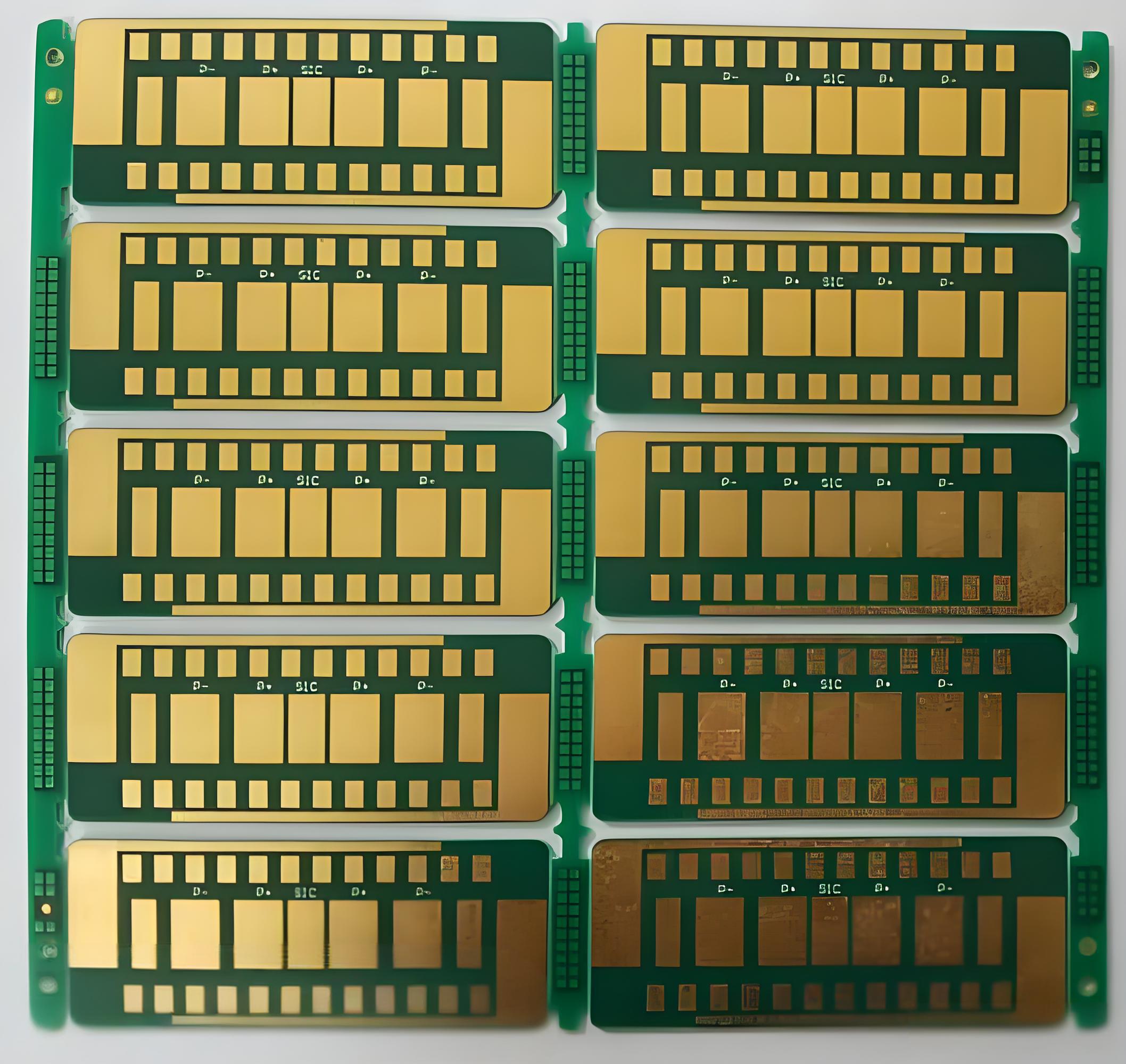
1. Open copper bearings
Open copper bearings are the most widely used copper type on any PCB. This is a metal area where the soldering components to the blackboard. With the design, they must remain open to allow solder to make a solid electrical and mechanical connection between tin components and PCB copper layers.
In addition to the component soldering, some open bearings are used for mechanical support or to connect the parts that produce heat to pour large copper for better heat dissipation. The right surface finishing on this bearing – such as hasl or enigâ € “helps prevent oxidation and increase solder capabilities.
2. Open Copper Traces
In some designs, traces (thin copper lines that connect different components) are deliberately left open. This is less common than open bearings, but is carried out in certain cases where designers need direct access to traces for testing or where traces carry high currents and the benefits of better heat dissipation.
One of the general uses for open copper traces is to make a test point. By leaving the trail found, engineers can place the probe directly on the trail during testing or problem solving.
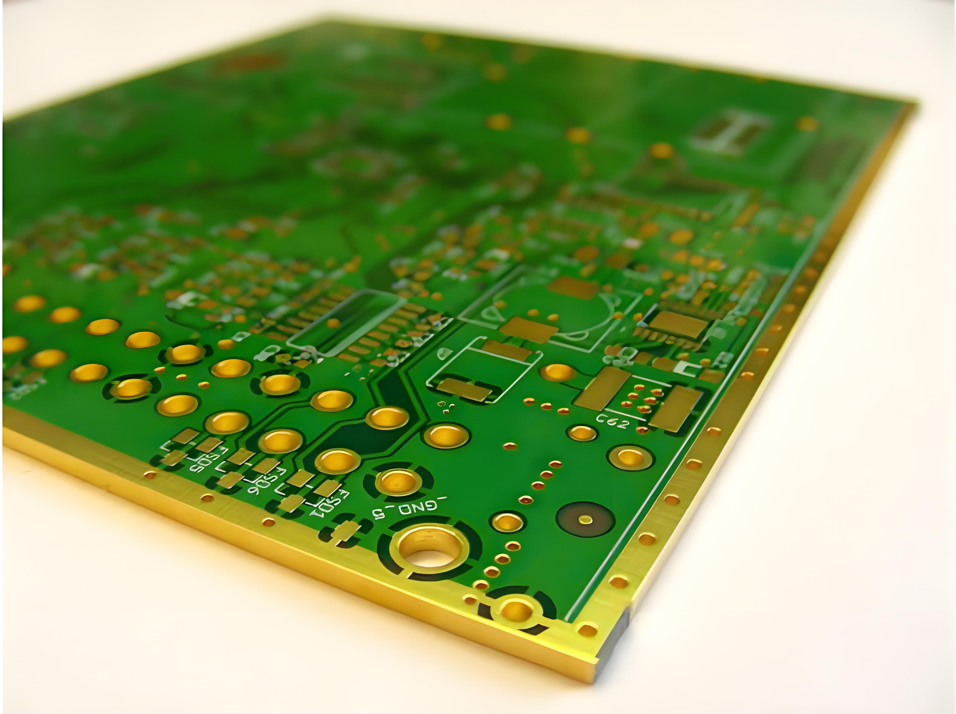
3. PCB Exposed Copper Edge
The copper edge exposed to PCB refers to copper that runs right to the edge of the PCB and remains exposed to functional use. This is usually found on a board that needs to be connected to the socket or other boards through the edge connectors. In this case, copper along the edge acts as a contact point and must remain exposed to a reliable electricity connection.
This type of open copper is also used for ground purposes. For example, in the RF circuit or high -speed digital design, the edge of the board may have exposed copper that is connected to the soil to reduce electromagnetic disorders (EMI). Some designs use edge coating, where copper is coated along the edge of the board to make a continuous conductive path.
What is the permit for copper to the edge of the PCB?
When designing a PCB, a copper-to-tepi permit is very important. Copper should not be placed too close to the edge unless it is intended to be exposed. If copper accidentally is too close to the edge, it can cause problems or manufacturing failures in the field.
Industrial Guidelines
Standard practice, according to IPC standards, recommends at least 0.25mm (10 miles) permission between copper and the edge of the board. This permit prevents copper from being damaged or exposed during cutting boards.
Edge copper design
If you design a PCB open copper edge, such as for connectors or earthing points, you can extend copper to the edges, but must be coated and processed correctly. Special instructions are needed for producers to jump over the edge and prevent delamination.
How do you design a PCB with an open copper plate?
Designing an open copper area requires the right planning and use of your PCB design software.
Step 1: Determine the copper area
Use copper pour, pads, or large planes for the area you want to open. Make sure they are connected to the correct net, either soil, power, or signal.
Step 2: Disable the soldering mask
In your PCB layout, deactivate mask solder above this area. This is done by making the opening of the solder mask in the relevant layer.
Step 3: edge exposure
For the PCB open copper edge design, spread copper to the edge of the board. Show this clearly in your mechanical image. Some producers need notes for edge plates.
Step 4: Selective Surface Selective
Decide whether copper will remain naked or have a final result such as HASL (Hot Air Solder Solder) or ENIG (Electric Nickel Soaking Gold). This final result prevents oxidation and increases endurance.
Risks and challenges with open copper PCBs
While the copper exposed to PCB serves many useful goals, it comes with challenges.
Oxidation and corrosion
Copper oxidizes rapidly in the air, forming a layer of brown or dull green. This can reduce conductivity and make solder difficult. Moist environment speeds up this process.
Short circuit
Open copper is more likely to cause shorts when touching other metal objects. Extra maintenance is needed in the design and assembly to avoid accidental contact.
Handling risk
The naked copper area can be scratched or contaminated during treatment. Fingerprints, dust, or humidity can affect performance. Careful protective and assembly packaging helps reduce this risk.
Copper design guidelines exposed in PCB layout
Here are some useful tips for designing an open copper area safely:
- Maintaining permits from high voltage areas unless insulation is provided.
- Use a protective coating like a conformal layer if the board will be exposed to a hard environment.
- Show clearly the copper area that is open in the Gerber file and your fabrication record.
- For the edge of the PCB open copper, it works with your manufacturer to ensure proper coating and endurance.
- Use thicker copper (for example, 2 ounces) for large open areas intended for heat or high current dissipation.
FAQ
1. How do I remove copper from the PCB board?
Copper can be eliminated through chemicals using ferric chloride or similar solutions. This can also be eroded mechanically or ground with a CNC tool.
2. What happens with open copper?
Open copper is oxidized when exposed to air and humidity. This can affect electrical performance, so that the final layer or coating is often applied.
3. Can a copper PCB that is exposed to be used outdoors?
Not directly. Outdoor use requires additional protection, such as conformal layers, to prevent corrosion. Without protection, copper will decrease rapidly.
4. How to prevent oxidation in open copper areas?
Apply coatings such as OSP (Organic Sutderability Preservatives), clear varnish, or conformal layers. Using surface finishing such as Enig or Hasl also helps.
5. What is the best surface finish if I want partial copper to open?
ENIG and HASL can be applied selectively. Masking during the finishing process allows partial copper exposure if needed.
6. Is open copper safe for high voltage applications?
Not except the right distance and isolation is used. High voltage requires strict permission and protection to avoid arches or shorts.
7. What is the difference between open copper and the final layer coated?
Copper that is exposed does not have an additional layer, while the final layer of layers such as Enig or Hasl increases protection and improve performance.
Tag: PCB Open copper design, open copper on PCB, PCB Exposed Copper Edge
This entry was posted on Friday, August 1, 2025 at 18:49 and submitted under the best PCB, BestTPCB, FAQ, PCB News, PCB Technology. You can follow any response to this entry through RSS 2.0 bait. You can leave a response, or trackback from your own site.
Game Center
Game News
Review Film
Berita Olahraga
Lowongan Kerja
Berita Terkini
Berita Terbaru
Berita Teknologi
Seputar Teknologi
Berita Politik
Resep Masakan
Pendidikan
Berita Terkini
Berita Terkini
Berita Terkini
review anime
Gaming Center
Originally posted 2025-08-02 05:31:59.