Gold fingers are one of the most critical features on many circuit boards, especially those used in high reliability connections. Whether you are building a test interface, designing a PCIE card, or making an edge connector, understanding the beveling of gold fingers and the design of the coating is very important for durability and smooth performance.
Let’s explore everything about PCB gold fingers, beveling processes, and how to choose the right beveling angle for your board design.
What is a golden finger?
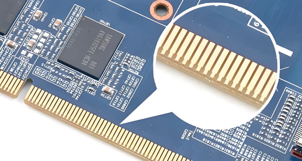
PCB gold fingers are gold -plated connectors located along the edge of the printed circuit board. They function as a contact point when the PCB is put into a slot or connector, such as in RAM, GPU card, or other modular systems. These fingers are coated with hard gold to make sure they can withstand the repetitive insertion and release cycle without fatigue.
They are called “fingers” because they look like narrow and elongated pads that stretch along the edge of the PCB, similar to the fingers. Every gold finger is connected to the circuit trail on the board. When the PCB is inserted into the slot, the metal contact on the gold fingers is parallel to the contact in the connector, allowing the signal to pass.
The main reason for gold is used is because it is not easily corrected easily. Gold provides high conductivity and can withstand many insertions without losing its shape or function. In a critical environment ”such as the military, aerospace, or telecommunications” ”reliability is very important.
Gold Finger Type on PCB
PCB gold fingers can be divided into two types -Multi -rise gold fingers and staggered gold fingers.
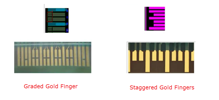
Multi -rise gold fingers refer to the design where the fingers are coated with gold at varying length or staggered height. Instead of all the fingers that are aligned in a straight line, some longer than the others. This is not only a visual variation € “This serves very specific goals. Multiple fingers are usually used in applications where controlling controlled insertions are needed. When PCB is inserted into a slot, the longer the fingers make contact first, followed by shorter ones.
Another design strategy uses long and short gold fingers also known as staggered gold fingers. This refers to the radius of gold with different physical lengths on the same edge, but usually without beveling or variations in the depth of coating. This technique is usually used in:
- PCIE Hot-Tluggable Cards
- Industrial control system with modules that can be replaced
- Burn-in equipment or tests that require a safe first contact
The length is designed based on the depth of the connector slot and how the PCB enters the socket. Sometimes only a few pins ‘like GND or VCC’ are made longer, while the rest remains short.
How thick is the PCB Gold Finger Plating?
The endurance of the golden fingers comes from their coating thickness. Not all gold fingers were created the same. The thickness of the coating affects how good performance is and how long they last.
Impure gold layer; This is an electroplated hard gold, which includes a little cobalt to increase worn out violence and resistance. Here are the details of the general thickness:
| Application type | The thickness of the gold coating (hard gold) |
| Standard consumer device | 0.76îlen (30îlen) |
| Industrial or light insertion | 1,27îlen (50îlen) |
| High power application | 2.54îief (100îief) |
In general, 50îief is the most common for boards that are plugged in and revoked many times. If the finger is not intended to be eliminated frequently, thinner coating is usually good. But when hesitant, thicker betterâ € “gives a stronger wear resistance.
What is the process of gold coating on the PCB?
Making a strong and reliable PCB gold finger requires precision. The coating process is carried out after the remaining board is made and cleaned. The focus is on adding a hard layer of gold only to the fingers’ not anywhere else.
1. Isolation of the finger area
First, the PCB is cleaned, and only the area of the finger is exposed. The remaining board is closed to prevent unwanted coating elsewhere.
2. Nickel coating (lower layer)
The nickel layer (usually 3â € “6îief) is electroplated to the copper finger base. Nickel increases the adhesion of gold and acts as a barrier to prevent copper from spreading into gold from time to time.
3. Gold Electroplating (top layer)
After the nickel, the hard layer of gold layered on it. This layer is usually between 30îief and 100îiefin depending on the application. The coating uses the current that pushes gold ions to the nickel surface.
4. Cleaning and Inspection
After the coating is complete, the board is cleaned, and the gold fingers are checked for uniformity, resistance, or lost areas.
5. Beveling (if needed)
If beveling is needed, it is done after the coating. The edges are formed to allow easier insertion to the connector.
6. The last finishing
The rest of the PCB receives the final result (for example, Enig, OSP, Hasl), but the gold fingers remain untouched.
This coating method produces long and smooth connectors that hold oxidation and mechanical wear.
What is a gold finger beveling?
Gold finger beveling is a mechanical process that cuts the edge of the PCB ‘where the golden fingers are in the tilted angle. Instead of the edge of 90 ° blunt, the bevel creates a surface like a smooth ramp.
Imagine shifting the PCB to the connector. The sharp edges may capture, damage the connector, or erode the coating. But the sloping edge glides smoothly, reduce friction and increase contact.
This is very useful for PCB used in:
- Backplane system
- Server rack
- Communication Module
- Plug-and-play component
Beveling processes are usually carried out using CNC milling or grinding precision. Treatment is taken to maintain the right angle measurement without defeating the gold coating.
The purpose of the beveling of gold fingers
There are several important reasons why beveling is applied to PCB gold fingers:
The sloping edge helps the PCB slide to the connector smoothly. This reduces the possibility of misalignment or traffic jam.
Without beveling, the sharp edge of the PCB can scratch the connector pin, causing problems with wear or initial performance.
Repeated insertion cycles can make gold coating. Beveling distributes more even pressure, extending the life of the board and connector.
- Better electrical contact
A smoother insertion means better alignment and tighter contact with a metal pin in the slot. This causes a more stable signal and fewer connection errors.
- Finishing Professional Manufacturing
The tilted gold radius looks smoother, indicating the work of high-quality PCB.
For any board that will be often deleted and often re -put, beveling is not just a good idea ‘that is almost important.
Beveling Gold Finger Angle Option
When beveling, you have an option for the bevel corner. The choice depends on how the PCB matches the slot and the level of strength of the insertion you want to reduce. Here is a common beveling angle:
| Corner | Information |
| 30 ° | The most popular angle. Balancing mechanical strength and ease of insertion. |
| 40 ° | Offers a smoother slope than 30 °. Used when insertion must be soft. |
| 45He | The most steep slope. Useful when the board has to slide into a slot with minimal resistance. |
Most applications remain with 30 °, but you must always check the specifications of the connector. Some high -speed or high -speed connectors may require tighter tolerance and smoother entrance paths.
Consideration of italics
Before you finish your beveling angle, consider the following:
Look at how your connector or socket is formed. If a narrow slot opening, a steeper bevel (like 45 °) might help.
If the PCB will be deleted frequently, as in the modular testing or settings, the smoother entry reduces long -term damage.
Bevel Sharper deletes more material. If the edge of your board carries a mechanical load, avoid bevel that is too steep.
The beveling process should not cut gold. Make sure the thickness of the gold coating is enough to cover the entire bevel.
See IPC-6012 and IPC-A-600 for Gold Finger Design Guidelines, Coating, and Beveling Requirements.
Always coordinate with your PCB manufacturer to ensure the chosen bevel angle is feasible and in accordance with the functional needs of your product.
Gold Fingers PCB Application
Gold fingers are everywhere. Any device that uses the edge connector is likely to have it. Some of the most common cases of use include:
- Graphic Card (GPU) – to connect with the motherboard
- RAM Module – Put in Dimm Slot
- Motherboard and backplanes – for communication between layers or devices
- Test interface boards-for Burn-in, Programming, or Debugging
- PLC and Industrial Control System-For Plug-in Module
- Medical Electronics and Defense – where reliability is very important
In all of these applications, beveling gold fingers help make sure the board does not fail during connection or release. This may look like small details, but its effect on reliability is very large. Gold finger beveling is one of the small but strong features that increases mechanical suitability, electrical contact, and the overall durability of your circuit board. When designing your next PCB, pay attention to:
- The thickness of the gold finger coating
- Whether beveling is needed
- The best angle for fine insertion
- And the wear of the board will experience
These decisions affect not only how well the council works, but how long it takes.
About the best technology
In the best technology, we specialize in PCB manufacturing with a focus on high reliability boards. We handle everything, ranging from hard gold finger design to beveling precision, ensuring your edge connectors meet international standards. Our team works with industries including medical, automotive, derivative, and telecommunications.
We follow the strict quality process and use the mes lacked system to track every step. Whether you need a fast prototype or high volume production, our engineer is ready to help you design, test, and provide high-performance PCB with long-lasting gold fingers.
Looking for PCB manufacturers who understand the details? Let’s build your next project together.
FAQ
1. Can I design a gold finger without beveling?
Yes, but for whatever board will be plugged in and out regularly, beveling is highly recommended for smoother installation and longer life.
2. What is the difference between Enig and Hard Gold?
Enig is used in pads for soldering. Hard gold -coated gold for wear resistance. They are different in composition and use.
3. How to determine beveling in my Gerber file?
You must include a separate image or mechanical notation in a fabrication note to show beveling angles and location.
4. Is the gold finger more expensive to produce?
Yes, because of the electroplating process and the cost of gold. However, they added a significant durability and value.
5. Can a tired golden finger coating?
Over time, yesâ € ”especially if the coating is thin. Using thicker coating like 50îief or more helps to prevent this.
Tag: Beveling Gold Finger
This entry was posted on Tuesday, July 8, 2025 at 18:30 and submitted under the best PCB, BestTPCB, Design Guide, FAQ, FR4 PCB, PCB Technology. You can follow any response to this entry through RSS 2.0 bait. You can leave a response, or trackback from your own site.
Game Center
Game News
Review Film
Berita Olahraga
Lowongan Kerja
Berita Terkini
Berita Terbaru
Berita Teknologi
Seputar Teknologi
Berita Politik
Resep Masakan
Pendidikan
Berita Terkini
Berita Terkini
Berita Terkini
review anime
Gaming Center
Originally posted 2025-07-10 14:25:21.